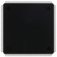
MCF5407AI220 Freescale Semiconductor, MCF5407AI220 Datasheet - Page 327

MCF5407AI220
Manufacturer Part Number
MCF5407AI220
Description
IC MPU 32B 220MHZ COLDF 208-FQFP
Manufacturer
Freescale Semiconductor
Series
MCF540xr
Specifications of MCF5407AI220
Core Processor
Coldfire V4
Core Size
32-Bit
Speed
220MHz
Connectivity
EBI/EMI, I²C, UART/USART
Peripherals
DMA, WDT
Number Of I /o
16
Program Memory Type
ROMless
Ram Size
4K x 8
Voltage - Supply (vcc/vdd)
1.65 V ~ 3.6 V
Oscillator Type
External
Operating Temperature
0°C ~ 70°C
Package / Case
208-FQFP
Maximum Clock Frequency
220 MHz
Operating Supply Voltage
1.8 V, 3.3 V
Maximum Operating Temperature
+ 105 C
Mounting Style
SMD/SMT
Minimum Operating Temperature
0 C
Program Memory Size
24KB
Cpu Speed
220MHz
Embedded Interface Type
I2C, UART
Digital Ic Case Style
FQFP
No. Of Pins
208
Supply Voltage Range
3.3V
Rohs Compliant
Yes
For Use With
M5407C3 - KIT EVAL FOR MCF5407 W/ETHERNET
Lead Free Status / RoHS Status
Lead free / RoHS Compliant
Eeprom Size
-
Program Memory Size
-
Data Converters
-
Lead Free Status / Rohs Status
Lead free / RoHS Compliant
Available stocks
Company
Part Number
Manufacturer
Quantity
Price
Company:
Part Number:
MCF5407AI220
Manufacturer:
freescaie
Quantity:
6
Company:
Part Number:
MCF5407AI220
Manufacturer:
Freescale Semiconductor
Quantity:
135
Company:
Part Number:
MCF5407AI220
Manufacturer:
FREESCALE
Quantity:
1 831
Company:
Part Number:
MCF5407AI220
Manufacturer:
Freescale Semiconductor
Quantity:
10 000
- Current page: 327 of 546
- Download datasheet (7Mb)
Although Figure 12-11 does not show TM0/DACK0 signaling a DMA acknowledgement,
this signal can provide an external request acknowledge response, as shown in subsequent
diagrams.
To initiate a request, DREQ need only be asserted long enough to be sampled on one rising
clock edge. However, note the following regarding the negation of DREQ:
Figure 12-12 shows a dual-address, peripheral-to-SDRAM DMA transfer. The DMA is not
parked on the bus, so the diagram shows how the CPU can generate multiple bus cycles
during DMA transfers. It also shows TM0/DACK0 timing. The TT signals indicate whether
the CPU (0) or DMA (1) has bus mastership. TM2 indicates dual-address mode.
If DCR[AT] is 1, TM/DACK is asserted during the final transfer. If DCR[AT] is 0,
TM/DACK asserts during all DMA accesses.
• In cycle-steal mode (DCR[CS] = 1), the read/write transaction is limited to a single
• In burst mode, (DCR[CS] = 0), multiple read/write transfers can occur on the bus as
TM0/DACK0
transfer. DREQ must be negated appropriately to avoid generating another request.
— For dual-address transfers, DREQ must be negated before TS is asserted for the
— For single-address transfers, DREQ must be negated before TS is asserted for the
programmed. DREQ need not be negated until DSR[DONE] is set, indicating the
block transfer is complete. Another transfer cannot be initiated until the DMA
registers are reprogrammed.
Figure 12-11. DREQ Timing Constraints, Dual-Address DMA Transfer
DREQ0
A[31:0]
CLKIN
write portion, as shown in Figure 12-11, clock cycle 7.
transfer, as shown in Figure 12-13, clock cycle 4.
R/W
TT1
TT0
CS
TS
TA
0
1
Chapter 12. DMA Controller Module
2
3
4
5
DMA Controller Module Functional Description
Read
6
7
8
9
Write
10
11
12-15
Related parts for MCF5407AI220
Image
Part Number
Description
Manufacturer
Datasheet
Request
R
Part Number:
Description:
Mcf5407 Coldfire Integrated Microprocessor User
Manufacturer:
Freescale Semiconductor, Inc
Datasheet:
Part Number:
Description:
Manufacturer:
Freescale Semiconductor, Inc
Datasheet:
Part Number:
Description:
Manufacturer:
Freescale Semiconductor, Inc
Datasheet:
Part Number:
Description:
Manufacturer:
Freescale Semiconductor, Inc
Datasheet:
Part Number:
Description:
Manufacturer:
Freescale Semiconductor, Inc
Datasheet:
Part Number:
Description:
Manufacturer:
Freescale Semiconductor, Inc
Datasheet:
Part Number:
Description:
Manufacturer:
Freescale Semiconductor, Inc
Datasheet:
Part Number:
Description:
Manufacturer:
Freescale Semiconductor, Inc
Datasheet:
Part Number:
Description:
Manufacturer:
Freescale Semiconductor, Inc
Datasheet:
Part Number:
Description:
Manufacturer:
Freescale Semiconductor, Inc
Datasheet:
Part Number:
Description:
Manufacturer:
Freescale Semiconductor, Inc
Datasheet:
Part Number:
Description:
Manufacturer:
Freescale Semiconductor, Inc
Datasheet:
Part Number:
Description:
Manufacturer:
Freescale Semiconductor, Inc
Datasheet:
Part Number:
Description:
Manufacturer:
Freescale Semiconductor, Inc
Datasheet:
Part Number:
Description:
Manufacturer:
Freescale Semiconductor, Inc
Datasheet:


