AT90PWM1-16SU Atmel, AT90PWM1-16SU Datasheet - Page 118
AT90PWM1-16SU
Manufacturer Part Number
AT90PWM1-16SU
Description
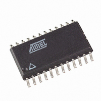
MCU AVR 8K FLASH 16MHZ 24-SOIC
Manufacturer
Atmel
Series
AVR® 90PWM Lightingr
Datasheet
1.AT90PWM1-16SU.pdf
(297 pages)
Specifications of AT90PWM1-16SU
Core Processor
AVR
Core Size
8-Bit
Speed
16MHz
Connectivity
SPI
Peripherals
Brown-out Detect/Reset, POR, PWM, WDT
Number Of I /o
19
Program Memory Size
8KB (8K x 8)
Program Memory Type
FLASH
Eeprom Size
512 x 8
Ram Size
512 x 8
Voltage - Supply (vcc/vdd)
2.7 V ~ 5.5 V
Data Converters
A/D 8x10b
Oscillator Type
Internal
Operating Temperature
-40°C ~ 105°C
Package / Case
24-SOIC (7.5mm Width)
Processor Series
AT90PWMx
Core
AVR8
Data Bus Width
8 bit
Data Ram Size
512 B
Interface Type
SPI
Maximum Clock Frequency
16 MHz
Number Of Programmable I/os
19
Number Of Timers
2
Maximum Operating Temperature
+ 105 C
Mounting Style
SMD/SMT
3rd Party Development Tools
EWAVR, EWAVR-BL
Development Tools By Supplier
ATAVRDRAGON, ATSTK500, ATSTK600, ATAVRISP2, ATAVRONEKIT, ATAVRFBKIT, ATAVRISP2
Minimum Operating Temperature
- 40 C
On-chip Adc
10 bit, 11 Channel
For Use With
ATSTK600-SOIC - STK600 SOCKET/ADAPTER FOR SOIC
Lead Free Status / RoHS Status
Lead free / RoHS Compliant
Available stocks
Company
Part Number
Manufacturer
Quantity
Price

Part Number:
AT90PWM1-16SU
Manufacturer:
ATMEL/爱特梅尔
Quantity:
20 000


Table 32. Waveform Generation Mode Bit Description
Note:
15.10.2
118
Mode
10
11
12
13
14
15
0
1
2
3
4
5
6
7
8
9
1. The CTCn and PWMn1:0 bit definition names are obsolete. Use the
AT90PWM1
WGMn3
Timer/Counter1 Control Register B – TCCR1B
location of these bits are compatible with previous versions of the timer.
0
0
0
0
0
0
0
0
1
1
1
1
1
1
1
1
WGMn2
(CTCn)
0
0
0
0
1
1
1
1
0
0
0
0
1
1
1
1
Note:
• Bit 1:0 – WGMn1:0: Waveform Generation Mode
Combined with the WGMn3:2 bits found in the TCCRnB Register, these bits control the counting
sequence of the counter, the source for maximum (TOP) counter value, and what type of wave-
form generation to be used, see
unit are: Normal mode (counter), Clear Timer on Compare match (CTC) mode, and three types
of Pulse Width Modulation (PWM) modes.
• Bit 7 – ICNCn: Input Capture Noise Canceler
Setting this bit (to one) activates the Input Capture Noise Canceler. When the noise canceler is
activated, the input from the Input Capture pin (ICPn) is filtered. The filter function requires four
successive equal valued samples of the ICPn pin for changing its output. The Input Capture is
therefore delayed by four Oscillator cycles when the noise canceler is enabled.
• Bit 6 – ICESn: Input Capture Edge Select
Bit
Read/Write
Initial Value
(PWMn1)
WGMn1
1. A special case occurs when OCRnA/OCRnB equals TOP and COMnA1/COMnB1 is set.
0
0
1
1
0
0
1
1
0
0
1
1
0
0
1
1
“Phase Correct PWM Mode” on page 111.
ICNC1
R/W
7
0
(PWMn0)
WGMn0
0
1
0
1
0
1
0
1
0
1
0
1
0
1
0
1
ICES1
R/W
6
0
(1)
Timer/Counter Mode of
Operation
Normal
PWM, Phase Correct, 8-bit
PWM, Phase Correct, 9-bit
PWM, Phase Correct, 10-bit
CTC
Fast PWM, 8-bit
Fast PWM, 9-bit
Fast PWM, 10-bit
PWM, Phase and Frequency
Correct
PWM, Phase and Frequency
Correct
PWM, Phase Correct
PWM, Phase Correct
CTC
(Reserved)
Fast PWM
Fast PWM
Table
R
5
–
0
32. Modes of operation supported by the Timer/Counter
WGM13
(See “16-bit Timer/Counter1 with PWM” on page
R/W
4
0
WGM
for more details.
WGM12
R/W
n2:0 definitions. However, the functionality and
3
0
TOP
0xFFFF
0x00FF
0x01FF
0x03FF
OCRnA
0x00FF
0x01FF
0x03FF
ICRn
OCRnA
ICRn
OCRnA
ICRn
–
ICRn
OCRnA
CS12
R/W
2
0
CS11
R/W
Update of
OCRn
Immediate
TOP
TOP
TOP
Immediate
TOP
TOP
TOP
BOTTOM
BOTTOM
TOP
TOP
Immediate
–
TOP
TOP
1
0
x
at
CS10
R/W
0
0
4378C–AVR–09/08
TOVn Flag
Set on
MAX
BOTTOM
BOTTOM
BOTTOM
MAX
TOP
TOP
TOP
BOTTOM
BOTTOM
BOTTOM
BOTTOM
MAX
–
TOP
TOP
TCCR1B
96.).
See
Related parts for AT90PWM1-16SU
Image
Part Number
Description
Manufacturer
Datasheet
Request
R

Part Number:
Description:
Manufacturer:
Atmel Corporation
Datasheet:

Part Number:
Description:
IC AVR PWM 8KB FLASH 16MHZ 32QFN
Manufacturer:
Atmel
Datasheet:

Part Number:
Description:
DEV KIT FOR AVR/AVR32
Manufacturer:
Atmel
Datasheet:
Part Number:
Description:
INTERVAL AND WIPE/WASH WIPER CONTROL IC WITH DELAY
Manufacturer:
ATMEL Corporation
Datasheet:
Part Number:
Description:
Low-Voltage Voice-Switched IC for Hands-Free Operation
Manufacturer:
ATMEL Corporation
Datasheet:
Part Number:
Description:
MONOLITHIC INTEGRATED FEATUREPHONE CIRCUIT
Manufacturer:
ATMEL Corporation
Datasheet:
Part Number:
Description:
AM-FM Receiver IC U4255BM-M
Manufacturer:
ATMEL Corporation
Datasheet:
Part Number:
Description:
Monolithic Integrated Feature Phone Circuit
Manufacturer:
ATMEL Corporation
Datasheet:
Part Number:
Description:
Multistandard Video-IF and Quasi Parallel Sound Processing
Manufacturer:
ATMEL Corporation
Datasheet:
Part Number:
Description:
High-performance EE PLD
Manufacturer:
ATMEL Corporation
Datasheet:
Part Number:
Description:
8-bit Flash Microcontroller
Manufacturer:
ATMEL Corporation
Datasheet: