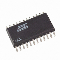
AT90PWM1-16SU Atmel, AT90PWM1-16SU Datasheet - Page 233
AT90PWM1-16SU
Manufacturer Part Number
AT90PWM1-16SU
Description
MCU AVR 8K FLASH 16MHZ 24-SOIC
Manufacturer
Atmel
Series
AVR® 90PWM Lightingr
Datasheet
1.AT90PWM1-16SU.pdf
(297 pages)
Specifications of AT90PWM1-16SU
Core Processor
AVR
Core Size
8-Bit
Speed
16MHz
Connectivity
SPI
Peripherals
Brown-out Detect/Reset, POR, PWM, WDT
Number Of I /o
19
Program Memory Size
8KB (8K x 8)
Program Memory Type
FLASH
Eeprom Size
512 x 8
Ram Size
512 x 8
Voltage - Supply (vcc/vdd)
2.7 V ~ 5.5 V
Data Converters
A/D 8x10b
Oscillator Type
Internal
Operating Temperature
-40°C ~ 105°C
Package / Case
24-SOIC (7.5mm Width)
Processor Series
AT90PWMx
Core
AVR8
Data Bus Width
8 bit
Data Ram Size
512 B
Interface Type
SPI
Maximum Clock Frequency
16 MHz
Number Of Programmable I/os
19
Number Of Timers
2
Maximum Operating Temperature
+ 105 C
Mounting Style
SMD/SMT
3rd Party Development Tools
EWAVR, EWAVR-BL
Development Tools By Supplier
ATAVRDRAGON, ATSTK500, ATSTK600, ATAVRISP2, ATAVRONEKIT, ATAVRFBKIT, ATAVRISP2
Minimum Operating Temperature
- 40 C
On-chip Adc
10 bit, 11 Channel
For Use With
ATSTK600-SOIC - STK600 SOCKET/ADAPTER FOR SOIC
Lead Free Status / RoHS Status
Lead free / RoHS Compliant
Available stocks
Company
Part Number
Manufacturer
Quantity
Price

Part Number:
AT90PWM1-16SU
Manufacturer:
ATMEL/爱特梅尔
Quantity:
20 000


4378C–AVR–09/08
Figure 22-9. Parallel Programming Timing, Reading Sequence (within the Same Page) with
Note:
Table 86. Parallel Programming Characteristics, V
Symbol
V
I
t
t
t
t
t
t
t
t
t
t
t
t
t
t
t
t
t
t
PP
DVXH
XLXH
XHXL
XLDX
XLWL
XLPH
PLXH
BVPH
PHPL
PLBX
WLBX
PLWL
BVWL
WLWH
WLRL
WLRH
WLRH_CE
XLOL
PP
XTAL1
DATA
BS1
XA0
XA1
OE
1. The timing requirements shown in
ing operation.
Parameter
Programming Enable Voltage
Programming Enable Current
Data and Control Valid before XTAL1 High
XTAL1 Low to XTAL1 High
XTAL1 Pulse Width High
Data and Control Hold after XTAL1 Low
XTAL1 Low to WR Low
XTAL1 Low to PAGEL high
PAGEL low to XTAL1 high
BS1 Valid before PAGEL High
PAGEL Pulse Width High
BS1 Hold after PAGEL Low
BS2/1 Hold after WR Low
PAGEL Low to WR Low
BS1 Valid to WR Low
WR Pulse Width Low
WR Low to RDY/BSY Low
WR Low to RDY/BSY High
WR Low to RDY/BSY High for Chip Erase
XTAL1 Low to OE Low
Timing Requirements
ADDR0 (Low Byte)
LOAD ADDRESS
(LOW BYTE)
t
XLOL
t
OLDV
(1)
(1)
DATA (Low Byte)
READ DATA
(LOW BYTE)
Figure 22-7
CC
t
BVDV
(2)
(i.e., t
= 5V ± 10%
DVXH
(HIGH BYTE)
READ DATA
DATA (High Byte)
, t
XHXL
Min
11.5
200
150
150
150
150
3.7
7.5
67
67
67
67
67
67
67
0
0
0
0
, and t
t
OHDZ
Typ
AT90PWM1
XLDX
LOAD ADDRESS
(LOW BYTE)
) also apply to read-
ADDR1 (Low Byte)
Max
12.5
250
4.5
1
9
Units
ms
ms
μA
μs
ns
ns
ns
ns
ns
ns
ns
ns
ns
ns
ns
ns
ns
ns
ns
V
233
Related parts for AT90PWM1-16SU
Image
Part Number
Description
Manufacturer
Datasheet
Request
R

Part Number:
Description:
Manufacturer:
Atmel Corporation
Datasheet:

Part Number:
Description:
IC AVR PWM 8KB FLASH 16MHZ 32QFN
Manufacturer:
Atmel
Datasheet:

Part Number:
Description:
DEV KIT FOR AVR/AVR32
Manufacturer:
Atmel
Datasheet:
Part Number:
Description:
INTERVAL AND WIPE/WASH WIPER CONTROL IC WITH DELAY
Manufacturer:
ATMEL Corporation
Datasheet:
Part Number:
Description:
Low-Voltage Voice-Switched IC for Hands-Free Operation
Manufacturer:
ATMEL Corporation
Datasheet:
Part Number:
Description:
MONOLITHIC INTEGRATED FEATUREPHONE CIRCUIT
Manufacturer:
ATMEL Corporation
Datasheet:
Part Number:
Description:
AM-FM Receiver IC U4255BM-M
Manufacturer:
ATMEL Corporation
Datasheet:
Part Number:
Description:
Monolithic Integrated Feature Phone Circuit
Manufacturer:
ATMEL Corporation
Datasheet:
Part Number:
Description:
Multistandard Video-IF and Quasi Parallel Sound Processing
Manufacturer:
ATMEL Corporation
Datasheet:
Part Number:
Description:
High-performance EE PLD
Manufacturer:
ATMEL Corporation
Datasheet:
Part Number:
Description:
8-bit Flash Microcontroller
Manufacturer:
ATMEL Corporation
Datasheet: