AT90PWM1-16SU Atmel, AT90PWM1-16SU Datasheet - Page 280
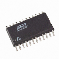
AT90PWM1-16SU
Manufacturer Part Number
AT90PWM1-16SU
Description
MCU AVR 8K FLASH 16MHZ 24-SOIC
Manufacturer
Atmel
Series
AVR® 90PWM Lightingr
Datasheet
1.AT90PWM1-16SU.pdf
(297 pages)
Specifications of AT90PWM1-16SU
Core Processor
AVR
Core Size
8-Bit
Speed
16MHz
Connectivity
SPI
Peripherals
Brown-out Detect/Reset, POR, PWM, WDT
Number Of I /o
19
Program Memory Size
8KB (8K x 8)
Program Memory Type
FLASH
Eeprom Size
512 x 8
Ram Size
512 x 8
Voltage - Supply (vcc/vdd)
2.7 V ~ 5.5 V
Data Converters
A/D 8x10b
Oscillator Type
Internal
Operating Temperature
-40°C ~ 105°C
Package / Case
24-SOIC (7.5mm Width)
Processor Series
AT90PWMx
Core
AVR8
Data Bus Width
8 bit
Data Ram Size
512 B
Interface Type
SPI
Maximum Clock Frequency
16 MHz
Number Of Programmable I/os
19
Number Of Timers
2
Maximum Operating Temperature
+ 105 C
Mounting Style
SMD/SMT
3rd Party Development Tools
EWAVR, EWAVR-BL
Development Tools By Supplier
ATAVRDRAGON, ATSTK500, ATSTK600, ATAVRISP2, ATAVRONEKIT, ATAVRFBKIT, ATAVRISP2
Minimum Operating Temperature
- 40 C
On-chip Adc
10 bit, 11 Channel
For Use With
ATSTK600-SOIC - STK600 SOCKET/ADAPTER FOR SOIC
Lead Free Status / RoHS Status
Lead free / RoHS Compliant
Available stocks
Company
Part Number
Manufacturer
Quantity
Price

Part Number:
AT90PWM1-16SU
Manufacturer:
ATMEL/爱特梅尔
Quantity:
20 000


Note:
280
0x1A (0x3A)
0x0E (0x2E)
0x0D (0x2D)
0x0C (0x2C)
0x0B (0x2B)
0x0A (0x2A)
0x19 (0x39)
0x18 (0x38)
0x17 (0x37)
0x16 (0x36)
0x15 (0x35)
0x14 (0x34)
0x13 (0x33)
0x12 (0x32)
0x11 (0x31)
0x10 (0x30)
0x0F (0x2F)
0x09 (0x29)
0x08 (0x28)
0x07 (0x27)
0x06 (0x26)
0x05 (0x25)
0x04 (0x24)
0x03 (0x23)
0x02 (0x22)
0x01 (0x21)
0x00 (0x20)
Address
1. For compatibility with future devices, reserved bits should be written to zero if accessed. Reserved I/O memory addresses
2. I/O Registers within the address range 0x00 - 0x1F are directly bit-accessible using the SBI and CBI instructions. In these
3. Some of the status flags are cleared by writing a logical one to them. Note that, unlike most other AVRs, the CBI and SBI
4. When using the I/O specific commands IN and OUT, the I/O addresses 0x00 - 0x3F must be used. When addressing I/O
AT90PWM1
should never be written.
registers, the value of single bits can be checked by using the SBIS and SBIC instructions.
instructions will only operate on the specified bit, and can therefore be used on registers containing such status flags. The
CBI and SBI instructions work with registers 0x00 to 0x1F only.
Registers as data space using LD and ST instructions, 0x20 must be added to these addresses. The AT90PWM1 is a com-
plex microcontroller with more peripheral units than can be supported within the 64 location reserved in Opcode for the IN
and OUT instructions. For the Extended I/O space from 0x60 - 0xFF in SRAM, only the ST/STS/STD and LD/LDS/LDD
instructions can be used.
Reserved
Reserved
Reserved
Reserved
Reserved
Reserved
Reserved
Reserved
Reserved
Reserved
Reserved
GPIOR2
GPIOR1
PORTE
PORTD
PORTB
Name
TIFR1
TIFR0
DDRE
DDRD
DDRB
PINE
PIND
PINB
–
–
–
GPIOR27
GPIOR17
PORTD7
PORTB7
PIND7
PINB7
DDD7
DDB7
Bit 7
–
–
–
–
–
–
–
–
–
–
–
–
–
–
–
–
–
–
–
GPIOR26
GPIOR16
PORTD6
PORTB6
PIND6
PINB6
DDD6
DDB6
Bit 6
–
–
–
–
–
–
–
–
–
–
–
–
–
–
–
–
–
–
–
GPIOR25
GPIOR15
PORTD5
PORTB5
PIND5
PINB5
DDD5
Bit 5
DDB5
ICF1
–
–
–
–
–
–
–
–
–
–
–
–
–
–
–
–
–
–
GPIOR24
GPIOR14
PORTD4
PORTB4
PIND4
PINB4
Bit 4
DDD4
DDB4
–
–
–
–
–
–
–
–
–
–
–
–
–
–
–
–
–
–
–
GPIOR23
GPIOR13
PORTD3
PORTB3
PIND3
PINB3
DDD3
DDB3
Bit 3
–
–
–
–
–
–
–
–
–
–
–
–
–
–
–
–
–
–
–
GPIOR22
GPIOR12
PORTD2
PORTE2
PORTB2
OCF1B
OCF0B
PINE2
PIND2
PINB2
DDE2
DDD2
DDB2
Bit 2
–
–
–
–
–
–
–
–
–
–
–
–
–
–
GPIOR21
GPIOR11
PORTE1
PORTD1
PORTB1
OCF1A
OCF0A
PIND1
PINE1
PINB1
DDE1
DDD1
DDB1
Bit 1
–
–
–
–
–
–
–
–
–
–
–
–
–
–
GPIOR20
GPIOR10
PORTE0
PORTD0
PORTB0
PINE0
PIND0
PINB0
DDE0
DDD0
DDB0
Bit 0
TOV1
TOV0
–
–
–
–
–
–
–
–
–
–
–
–
–
–
4378C–AVR–09/08
page 122
page 25
page 25
page 94
page 73
page 73
page 73
page 73
page 73
page 73
page 72
page 72
page 73
Page
–
–
–
Related parts for AT90PWM1-16SU
Image
Part Number
Description
Manufacturer
Datasheet
Request
R

Part Number:
Description:
Manufacturer:
Atmel Corporation
Datasheet:

Part Number:
Description:
IC AVR PWM 8KB FLASH 16MHZ 32QFN
Manufacturer:
Atmel
Datasheet:

Part Number:
Description:
DEV KIT FOR AVR/AVR32
Manufacturer:
Atmel
Datasheet:
Part Number:
Description:
INTERVAL AND WIPE/WASH WIPER CONTROL IC WITH DELAY
Manufacturer:
ATMEL Corporation
Datasheet:
Part Number:
Description:
Low-Voltage Voice-Switched IC for Hands-Free Operation
Manufacturer:
ATMEL Corporation
Datasheet:
Part Number:
Description:
MONOLITHIC INTEGRATED FEATUREPHONE CIRCUIT
Manufacturer:
ATMEL Corporation
Datasheet:
Part Number:
Description:
AM-FM Receiver IC U4255BM-M
Manufacturer:
ATMEL Corporation
Datasheet:
Part Number:
Description:
Monolithic Integrated Feature Phone Circuit
Manufacturer:
ATMEL Corporation
Datasheet:
Part Number:
Description:
Multistandard Video-IF and Quasi Parallel Sound Processing
Manufacturer:
ATMEL Corporation
Datasheet:
Part Number:
Description:
High-performance EE PLD
Manufacturer:
ATMEL Corporation
Datasheet:
Part Number:
Description:
8-bit Flash Microcontroller
Manufacturer:
ATMEL Corporation
Datasheet: