AT90PWM1-16SU Atmel, AT90PWM1-16SU Datasheet - Page 291
AT90PWM1-16SU
Manufacturer Part Number
AT90PWM1-16SU
Description
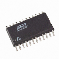
MCU AVR 8K FLASH 16MHZ 24-SOIC
Manufacturer
Atmel
Series
AVR® 90PWM Lightingr
Datasheet
1.AT90PWM1-16SU.pdf
(297 pages)
Specifications of AT90PWM1-16SU
Core Processor
AVR
Core Size
8-Bit
Speed
16MHz
Connectivity
SPI
Peripherals
Brown-out Detect/Reset, POR, PWM, WDT
Number Of I /o
19
Program Memory Size
8KB (8K x 8)
Program Memory Type
FLASH
Eeprom Size
512 x 8
Ram Size
512 x 8
Voltage - Supply (vcc/vdd)
2.7 V ~ 5.5 V
Data Converters
A/D 8x10b
Oscillator Type
Internal
Operating Temperature
-40°C ~ 105°C
Package / Case
24-SOIC (7.5mm Width)
Processor Series
AT90PWMx
Core
AVR8
Data Bus Width
8 bit
Data Ram Size
512 B
Interface Type
SPI
Maximum Clock Frequency
16 MHz
Number Of Programmable I/os
19
Number Of Timers
2
Maximum Operating Temperature
+ 105 C
Mounting Style
SMD/SMT
3rd Party Development Tools
EWAVR, EWAVR-BL
Development Tools By Supplier
ATAVRDRAGON, ATSTK500, ATSTK600, ATAVRISP2, ATAVRONEKIT, ATAVRFBKIT, ATAVRISP2
Minimum Operating Temperature
- 40 C
On-chip Adc
10 bit, 11 Channel
For Use With
ATSTK600-SOIC - STK600 SOCKET/ADAPTER FOR SOIC
Lead Free Status / RoHS Status
Lead free / RoHS Compliant
Available stocks
Company
Part Number
Manufacturer
Quantity
Price

Part Number:
AT90PWM1-16SU
Manufacturer:
ATMEL/爱特梅尔
Quantity:
20 000


Table of Contents
4378C–AVR–09/08
1
2
3
4
5
6
7
History ....................................................................................................... 2
Disclaimer ................................................................................................. 2
Pin Configurations ................................................................................... 2
Overview ................................................................................................... 5
AVR CPU Core .......................................................................................... 9
Memories ................................................................................................ 17
System Clock ......................................................................................... 27
3.1 Pin Descriptions .......................................................................................................4
4.1 Block Diagram .........................................................................................................6
4.2 Pin Descriptions .......................................................................................................7
4.3 About Code Examples .............................................................................................8
5.1 Introduction ..............................................................................................................9
5.2 Architectural Overview .............................................................................................9
5.3 ALU – Arithmetic Logic Unit ...................................................................................10
5.4 Status Register ......................................................................................................11
5.5 General Purpose Register File ..............................................................................12
5.6 Stack Pointer .........................................................................................................13
5.7 Instruction Execution Timing .................................................................................13
5.8 Reset and Interrupt Handling .................................................................................14
6.1 In-System Reprogrammable Flash Program Memory ...........................................17
6.2 SRAM Data Memory ..............................................................................................17
6.3 EEPROM Data Memory ........................................................................................19
6.4 I/O Memory ............................................................................................................25
6.5 General Purpose I/O Registers .............................................................................25
7.1 Clock Systems and their Distribution .....................................................................27
7.2 Clock Sources .......................................................................................................28
7.3 Default Clock Source .............................................................................................29
7.4 Low Power Crystal Oscillator .................................................................................29
7.5 Calibrated Internal RC Oscillator ...........................................................................30
7.6 PLL ........................................................................................................................32
7.7 128 kHz Internal Oscillator ....................................................................................34
7.8 External Clock .......................................................................................................34
AT90PWM1
291
Related parts for AT90PWM1-16SU
Image
Part Number
Description
Manufacturer
Datasheet
Request
R

Part Number:
Description:
Manufacturer:
Atmel Corporation
Datasheet:

Part Number:
Description:
IC AVR PWM 8KB FLASH 16MHZ 32QFN
Manufacturer:
Atmel
Datasheet:

Part Number:
Description:
DEV KIT FOR AVR/AVR32
Manufacturer:
Atmel
Datasheet:
Part Number:
Description:
INTERVAL AND WIPE/WASH WIPER CONTROL IC WITH DELAY
Manufacturer:
ATMEL Corporation
Datasheet:
Part Number:
Description:
Low-Voltage Voice-Switched IC for Hands-Free Operation
Manufacturer:
ATMEL Corporation
Datasheet:
Part Number:
Description:
MONOLITHIC INTEGRATED FEATUREPHONE CIRCUIT
Manufacturer:
ATMEL Corporation
Datasheet:
Part Number:
Description:
AM-FM Receiver IC U4255BM-M
Manufacturer:
ATMEL Corporation
Datasheet:
Part Number:
Description:
Monolithic Integrated Feature Phone Circuit
Manufacturer:
ATMEL Corporation
Datasheet:
Part Number:
Description:
Multistandard Video-IF and Quasi Parallel Sound Processing
Manufacturer:
ATMEL Corporation
Datasheet:
Part Number:
Description:
High-performance EE PLD
Manufacturer:
ATMEL Corporation
Datasheet:
Part Number:
Description:
8-bit Flash Microcontroller
Manufacturer:
ATMEL Corporation
Datasheet: