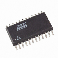
AT90PWM1-16SU Atmel, AT90PWM1-16SU Datasheet - Page 65
AT90PWM1-16SU
Manufacturer Part Number
AT90PWM1-16SU
Description
MCU AVR 8K FLASH 16MHZ 24-SOIC
Manufacturer
Atmel
Series
AVR® 90PWM Lightingr
Datasheet
1.AT90PWM1-16SU.pdf
(297 pages)
Specifications of AT90PWM1-16SU
Core Processor
AVR
Core Size
8-Bit
Speed
16MHz
Connectivity
SPI
Peripherals
Brown-out Detect/Reset, POR, PWM, WDT
Number Of I /o
19
Program Memory Size
8KB (8K x 8)
Program Memory Type
FLASH
Eeprom Size
512 x 8
Ram Size
512 x 8
Voltage - Supply (vcc/vdd)
2.7 V ~ 5.5 V
Data Converters
A/D 8x10b
Oscillator Type
Internal
Operating Temperature
-40°C ~ 105°C
Package / Case
24-SOIC (7.5mm Width)
Processor Series
AT90PWMx
Core
AVR8
Data Bus Width
8 bit
Data Ram Size
512 B
Interface Type
SPI
Maximum Clock Frequency
16 MHz
Number Of Programmable I/os
19
Number Of Timers
2
Maximum Operating Temperature
+ 105 C
Mounting Style
SMD/SMT
3rd Party Development Tools
EWAVR, EWAVR-BL
Development Tools By Supplier
ATAVRDRAGON, ATSTK500, ATSTK600, ATAVRISP2, ATAVRONEKIT, ATAVRFBKIT, ATAVRISP2
Minimum Operating Temperature
- 40 C
On-chip Adc
10 bit, 11 Channel
For Use With
ATSTK600-SOIC - STK600 SOCKET/ADAPTER FOR SOIC
Lead Free Status / RoHS Status
Lead free / RoHS Compliant
Available stocks
Company
Part Number
Manufacturer
Quantity
Price

Part Number:
AT90PWM1-16SU
Manufacturer:
ATMEL/爱特梅尔
Quantity:
20 000


11.3.1
11.3.2
4378C–AVR–09/08
MCU Control Register – MCUCR
Alternate Functions of Port B
• Bit 4 – PUD: Pull-up Disable
When this bit is written to one, the pull-ups in the I/O ports are disabled even if the DDxn and
PORTxn Registers are configured to enable the pull-ups ({DDxn, PORTxn} = 0b01). Se
The Port B pins with alternate functions are shown in
Table 9. Port B Pins Alternate Functions
The alternate pin configuration is as follows:
• PSCOUT01/ADC4/SCK – Bit 7
PSCOUT01: Output 1 of PSC 0.
ADC4, Analog to Digital Converter, input channel 4
SCK: Master Clock output, Slave Clock input pin for SPI channel. When the SPI is enabled as a
slave, this pin is configured as an input regardless of the setting of DDB7. When the SPI is
enabled as a master, the data direction of this pin is controlled by DDB7. When the pin is forced
to be an input, the pull-up can still be controlled by the PORTB7 bit.
• ADC7/ICP1B/PSCOUT11 – Bit 6
ADC7, Analog to Digital Converter, input channel 7
ICP1B, Input Capture Pin: The PB6 pin can act as an Input Capture Pin for Timer/Counter1.
PSCOUT11: Output 1 of PSC 1.
Bit
Read/Write
Initial Value
Port Pin
PB7
PB6
PB5
PB4
PB3
PB2
PB1
PB0
PSCOUT01 output
ADC4 (Analog Input Channel 4)
SCK (SPI Bus Serial Clock)
ADC7 (Analog Input Channel 7)
ICP1B (Timer 1 input capture alternate input)
PSCOUT11 output (see note 4)
ADC6 (Analog Input Channel 6)
INT2
ADC5 (Analog Input Channel5 )
INT1
MOSI (SPI Master Out Slave In)
PSCOUT21 output
MISO (SPI Master In Slave Out)
PSCOUT20 output
Alternate Functions
AMP0+ (Analog Differential Amplifier 0 Input Channel )
AMP0- (Analog Differential Amplifier 0 Input Channel )
SPIPS
R/W
7
0
R
6
–
0
R
5
–
0
PUD
R/W
4
0
.
.
Table
R
3
–
0
9.
R
2
–
0
IVSEL
R/W
1
0
AT90PWM1
IVCE
R/W
0
0
MCUCR
65
Related parts for AT90PWM1-16SU
Image
Part Number
Description
Manufacturer
Datasheet
Request
R

Part Number:
Description:
Manufacturer:
Atmel Corporation
Datasheet:

Part Number:
Description:
IC AVR PWM 8KB FLASH 16MHZ 32QFN
Manufacturer:
Atmel
Datasheet:

Part Number:
Description:
DEV KIT FOR AVR/AVR32
Manufacturer:
Atmel
Datasheet:
Part Number:
Description:
INTERVAL AND WIPE/WASH WIPER CONTROL IC WITH DELAY
Manufacturer:
ATMEL Corporation
Datasheet:
Part Number:
Description:
Low-Voltage Voice-Switched IC for Hands-Free Operation
Manufacturer:
ATMEL Corporation
Datasheet:
Part Number:
Description:
MONOLITHIC INTEGRATED FEATUREPHONE CIRCUIT
Manufacturer:
ATMEL Corporation
Datasheet:
Part Number:
Description:
AM-FM Receiver IC U4255BM-M
Manufacturer:
ATMEL Corporation
Datasheet:
Part Number:
Description:
Monolithic Integrated Feature Phone Circuit
Manufacturer:
ATMEL Corporation
Datasheet:
Part Number:
Description:
Multistandard Video-IF and Quasi Parallel Sound Processing
Manufacturer:
ATMEL Corporation
Datasheet:
Part Number:
Description:
High-performance EE PLD
Manufacturer:
ATMEL Corporation
Datasheet:
Part Number:
Description:
8-bit Flash Microcontroller
Manufacturer:
ATMEL Corporation
Datasheet: