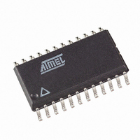
AT90PWM1-16SU Atmel, AT90PWM1-16SU Datasheet - Page 17

AT90PWM1-16SU
Manufacturer Part Number
AT90PWM1-16SU
Description
MCU AVR 8K FLASH 16MHZ 24-SOIC
Manufacturer
Atmel
Series
AVR® 90PWM Lightingr
Datasheet
1.AT90PWM1-16SU.pdf
(297 pages)
Specifications of AT90PWM1-16SU
Core Processor
AVR
Core Size
8-Bit
Speed
16MHz
Connectivity
SPI
Peripherals
Brown-out Detect/Reset, POR, PWM, WDT
Number Of I /o
19
Program Memory Size
8KB (8K x 8)
Program Memory Type
FLASH
Eeprom Size
512 x 8
Ram Size
512 x 8
Voltage - Supply (vcc/vdd)
2.7 V ~ 5.5 V
Data Converters
A/D 8x10b
Oscillator Type
Internal
Operating Temperature
-40°C ~ 105°C
Package / Case
24-SOIC (7.5mm Width)
Processor Series
AT90PWMx
Core
AVR8
Data Bus Width
8 bit
Data Ram Size
512 B
Interface Type
SPI
Maximum Clock Frequency
16 MHz
Number Of Programmable I/os
19
Number Of Timers
2
Maximum Operating Temperature
+ 105 C
Mounting Style
SMD/SMT
3rd Party Development Tools
EWAVR, EWAVR-BL
Development Tools By Supplier
ATAVRDRAGON, ATSTK500, ATSTK600, ATAVRISP2, ATAVRONEKIT, ATAVRFBKIT, ATAVRISP2
Minimum Operating Temperature
- 40 C
On-chip Adc
10 bit, 11 Channel
For Use With
ATSTK600-SOIC - STK600 SOCKET/ADAPTER FOR SOIC
Lead Free Status / RoHS Status
Lead free / RoHS Compliant
Available stocks
Company
Part Number
Manufacturer
Quantity
Price
Part Number:
AT90PWM1-16SU
Manufacturer:
ATMEL/爱特梅尔
Quantity:
20 000
- Current page: 17 of 297
- Download datasheet (4Mb)
6. Memories
6.1
6.2
4378C–AVR–09/08
In-System Reprogrammable Flash Program Memory
SRAM Data Memory
This section describes the different memories in the AT90PWM1. The AVR architecture has two
main memory spaces, the Data Memory and the Program Memory space. In addition, the
AT90PWM1 features an EEPROM Memory for data storage. All three memory spaces are linear
and regular.
The AT90PWM1 contains 8K bytes On-chip In-System Reprogrammable Flash memory for pro-
gram storage. Since all AVR instructions are 16 or 32 bits wide, the Flash is organized as 4K x
16. For software security, the Flash Program memory space is divided into two sections, Boot
Program section and Application Program section.
The Flash memory has an endurance of at least 10,000 write/erase cycles. The AT90PWM1
Program Counter (PC) is 12 bits wide, thus addressing the 4K program memory locations. The
operation of Boot Program section and associated Boot Lock bits for software protection are
described in detail in
205.
in SPI or Parallel programming mode.
Constant tables can be allocated within the entire program memory address space (see the LPM
– Load Program Memory.
Timing diagrams for instruction fetch and execution are presented in
ing” on page
Figure 1. Program Memory Map
Figure 2
“Memory Programming” on page 219
shows how the AT90PWM1 SRAM Memory is organized.
13.
“Boot Loader Support – Read-While-Write Self-Programming” on page
Application Flash Section
Boot Flash Section
Program Memory
contains a detailed description on Flash programming
0x0000
0x0FFF
“Instruction Execution Tim-
AT90PWM1
17
Related parts for AT90PWM1-16SU
Image
Part Number
Description
Manufacturer
Datasheet
Request
R

Part Number:
Description:
Manufacturer:
Atmel Corporation
Datasheet:

Part Number:
Description:
IC AVR PWM 8KB FLASH 16MHZ 32QFN
Manufacturer:
Atmel
Datasheet:

Part Number:
Description:
DEV KIT FOR AVR/AVR32
Manufacturer:
Atmel
Datasheet:

Part Number:
Description:
INTERVAL AND WIPE/WASH WIPER CONTROL IC WITH DELAY
Manufacturer:
ATMEL Corporation
Datasheet:

Part Number:
Description:
Low-Voltage Voice-Switched IC for Hands-Free Operation
Manufacturer:
ATMEL Corporation
Datasheet:

Part Number:
Description:
MONOLITHIC INTEGRATED FEATUREPHONE CIRCUIT
Manufacturer:
ATMEL Corporation
Datasheet:

Part Number:
Description:
AM-FM Receiver IC U4255BM-M
Manufacturer:
ATMEL Corporation
Datasheet:

Part Number:
Description:
Monolithic Integrated Feature Phone Circuit
Manufacturer:
ATMEL Corporation
Datasheet:

Part Number:
Description:
Multistandard Video-IF and Quasi Parallel Sound Processing
Manufacturer:
ATMEL Corporation
Datasheet:

Part Number:
Description:
High-performance EE PLD
Manufacturer:
ATMEL Corporation
Datasheet:

Part Number:
Description:
8-bit Flash Microcontroller
Manufacturer:
ATMEL Corporation
Datasheet:


