AT90PWM1-16SU Atmel, AT90PWM1-16SU Datasheet - Page 8
AT90PWM1-16SU
Manufacturer Part Number
AT90PWM1-16SU
Description
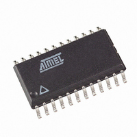
MCU AVR 8K FLASH 16MHZ 24-SOIC
Manufacturer
Atmel
Series
AVR® 90PWM Lightingr
Datasheet
1.AT90PWM1-16SU.pdf
(297 pages)
Specifications of AT90PWM1-16SU
Core Processor
AVR
Core Size
8-Bit
Speed
16MHz
Connectivity
SPI
Peripherals
Brown-out Detect/Reset, POR, PWM, WDT
Number Of I /o
19
Program Memory Size
8KB (8K x 8)
Program Memory Type
FLASH
Eeprom Size
512 x 8
Ram Size
512 x 8
Voltage - Supply (vcc/vdd)
2.7 V ~ 5.5 V
Data Converters
A/D 8x10b
Oscillator Type
Internal
Operating Temperature
-40°C ~ 105°C
Package / Case
24-SOIC (7.5mm Width)
Processor Series
AT90PWMx
Core
AVR8
Data Bus Width
8 bit
Data Ram Size
512 B
Interface Type
SPI
Maximum Clock Frequency
16 MHz
Number Of Programmable I/os
19
Number Of Timers
2
Maximum Operating Temperature
+ 105 C
Mounting Style
SMD/SMT
3rd Party Development Tools
EWAVR, EWAVR-BL
Development Tools By Supplier
ATAVRDRAGON, ATSTK500, ATSTK600, ATAVRISP2, ATAVRONEKIT, ATAVRFBKIT, ATAVRISP2
Minimum Operating Temperature
- 40 C
On-chip Adc
10 bit, 11 Channel
For Use With
ATSTK600-SOIC - STK600 SOCKET/ADAPTER FOR SOIC
Lead Free Status / RoHS Status
Lead free / RoHS Compliant
Available stocks
Company
Part Number
Manufacturer
Quantity
Price

Part Number:
AT90PWM1-16SU
Manufacturer:
ATMEL/爱特梅尔
Quantity:
20 000


4.2.5
4.2.6
4.2.7
4.3
8
About Code Examples
AT90PWM1
Port E (PE2..0) RESET/ XTAL1/
XTAL2
AVCC
AREF
Port E is an 3-bit bi-directional I/O port with internal pull-up resistors (selected for each bit). The
Port E output buffers have symmetrical drive characteristics with both high sink and source
capability. As inputs, Port E pins that are externally pulled low will source current if the pull-up
resistors are activated. The Port E pins are tri-stated when a reset condition becomes active,
even if the clock is not running.
If the RSTDISBL Fuse is programmed, PE0 is used as an I/O pin. Note that the electrical char-
acteristics of PE0 differ from those of the other pins of Port C.
If the RSTDISBL Fuse is unprogrammed, PE0 is used as a Reset input. A low level on this pin
for longer than the minimum pulse length will generate a Reset, even if the clock is not running.
The minimum pulse length is given in
to generate a Reset.
Depending on the clock selection fuse settings, PE1 can be used as input to the inverting Oscil-
lator amplifier and input to the internal clock operating circuit.
Depending on the clock selection fuse settings, PE2 can be used as output from the inverting
Oscillator amplifier.
The various special features of Port E are elaborated in
71
AVCC is the supply voltage pin for the A/D Converter on Port F. It should be externally con-
nected to V
through a low-pass filter.
This is the analog reference pin for the A/D Converter.
This documentation contains simple code examples that briefly show how to use various parts of
the device. These code examples assume that the part specific header file is included before
compilation. Be aware that not all C compiler vendors include bit definitions in the header files
and interrupt handling in C is compiler dependent. Please confirm with the C compiler documen-
tation for more details.
and
“Clock Systems and their Distribution” on page
CC
, even if the ADC is not used. If the ADC is used, it should be connected to V
Table 9-1 on page
27.
“Alternate Functions of Port E” on page
43. Shorter pulses are not guaranteed
4378C–AVR–09/08
CC
Related parts for AT90PWM1-16SU
Image
Part Number
Description
Manufacturer
Datasheet
Request
R

Part Number:
Description:
Manufacturer:
Atmel Corporation
Datasheet:

Part Number:
Description:
IC AVR PWM 8KB FLASH 16MHZ 32QFN
Manufacturer:
Atmel
Datasheet:

Part Number:
Description:
DEV KIT FOR AVR/AVR32
Manufacturer:
Atmel
Datasheet:
Part Number:
Description:
INTERVAL AND WIPE/WASH WIPER CONTROL IC WITH DELAY
Manufacturer:
ATMEL Corporation
Datasheet:
Part Number:
Description:
Low-Voltage Voice-Switched IC for Hands-Free Operation
Manufacturer:
ATMEL Corporation
Datasheet:
Part Number:
Description:
MONOLITHIC INTEGRATED FEATUREPHONE CIRCUIT
Manufacturer:
ATMEL Corporation
Datasheet:
Part Number:
Description:
AM-FM Receiver IC U4255BM-M
Manufacturer:
ATMEL Corporation
Datasheet:
Part Number:
Description:
Monolithic Integrated Feature Phone Circuit
Manufacturer:
ATMEL Corporation
Datasheet:
Part Number:
Description:
Multistandard Video-IF and Quasi Parallel Sound Processing
Manufacturer:
ATMEL Corporation
Datasheet:
Part Number:
Description:
High-performance EE PLD
Manufacturer:
ATMEL Corporation
Datasheet:
Part Number:
Description:
8-bit Flash Microcontroller
Manufacturer:
ATMEL Corporation
Datasheet: