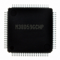
M38D59GCHP#U0 Renesas Electronics America, M38D59GCHP#U0 Datasheet - Page 128

M38D59GCHP#U0
Manufacturer Part Number
M38D59GCHP#U0
Description
IC 740/38D5 MCU QZ-ROM 80LQFP
Manufacturer
Renesas Electronics America
Series
740/38000r
Datasheet
1.M38D58G8FPU0.pdf
(144 pages)
Specifications of M38D59GCHP#U0
Core Processor
740
Core Size
8-Bit
Speed
12.5MHz
Connectivity
SIO, UART/USART
Peripherals
LCD, LED, PWM, WDT
Number Of I /o
59
Program Memory Size
48KB (48K x 8)
Program Memory Type
QzROM
Ram Size
2K x 8
Voltage - Supply (vcc/vdd)
1.8 V ~ 5.5 V
Data Converters
A/D 8x10b
Oscillator Type
Internal
Operating Temperature
-20°C ~ 85°C
Package / Case
80-LQFP
Lead Free Status / RoHS Status
Lead free / RoHS Compliant
Eeprom Size
-
Available stocks
Company
Part Number
Manufacturer
Quantity
Price
38D5 Group
Rev.3.04
REJ03B0158-0304
Notes on Timers
1. Frequency Divider
All timers shares one circuit for the frequency divider to generate
the count source.
Thus the frequency divider is not initialized when each
individual timer is activated. When the frequency divider is
selected as the count source, a one-cycle delay of the maximum
count source will result between when the timer is activated and
when it starts counting or outputs the waveform.
The count source cannot be observed externally.
2. Division Ratio for Timer 1 to 4
The division ratio is 1/(n+1) when the value n (0 to 255) is
written to the timer latch.
3. Switching Frequency and Count Source for Timer 1
Switch the frequency division or count source* while the timer
count is stopped.
*This also applies when the frequency divider output is selected
4. Setting Timer 1 and 2 When STP Instruction
Before executing the STP instruction, first set the wait time at
return.
5. Setting Order to Timer 1 to 4
When switching the count source of timer 1 to timer 4, a narrow
pulse may be generated at the count input, which causes the timer
count value to be undefined. Also, if the timers are used in
cascade connection, a narrow pulse may be generated at the
output when writing to the pervious timer, which causes the next
timer count value to be undefined.
Thus set the value from timer 1 in order after setting the count
source of timer 1 to timer 4.
6. Write to Timer 2, 3, and 4
When writing to the latch only, if the write timing to the reload
latch and the underflow timing are almost the same, the value is
set into the timer and the timer latch at the same time. At this
time, count is stopped during write operation to the reload latch.
7. Timer 3 PWM
(1) When PWM output is suspended once it starts, the time to
(2) When PWM mode is used, the interrupt requests and values
as the timer count source and the count source is switched in
conjunction with a transition between operating modes (on-
chip oscillator mode, X
careful when changing settings in the CPU mode register.
to 4, X, and Y
Executed
resume outputting may be delayed one section (256 × ts) of
the short interval depending on the level of the output pulse
at that time:
Stop at “H”: No output delay
Stop at “L”: Output is delayed time of 256 × ts
of timer 3 and timer 4 are updated every cycle of the long
interval (4 × 256 × ts).
May 20, 2008 Page 126 of 134
0
Mode, Timer 4 PWM
IN
mode, or low-speed mode). Be
1
Mode
8. Write Order to Timer X
(1) When timer mode, pulse output mode, event counter mode,
(2) Write to the timer X register by the 16-bit unit. Do not read
(3) When IGBT output mode or PWM mode is set, do not write
9. Read Order to Timer X
(1) In all modes, read the following registers in the order below:
(2) Read the timer X register in 16-bit units. Do not write to it
or pulse width measurement mode is set, write to the
following registers in the order below:
The timer X register (extension)
The timer X register (low-order)
The timer X register (high-order)
Writing to only one of these registers cannot be performed.
When either of the above modes is set and timer X operates
as a 16-bit counter, if the timer X register (extension) is never
set after a reset release, setting the timer X register
(extension) is not required. In that case, write the timer X
register (low-order) first and the timer X register (high-order)
next. However, once the timer X register (extension) is
written, note that the value is retained in the reload latch.
the timer X register while write operation is performed. If the
write operation is not completed, normal operation will not
be performed.
“1” to the timer X register (extension). If “1” has been
already written to the timer X register, be sure to write “0” to
the register before use.
Write to the following registers in the order below:
The compare registers 1, 2, 3 (high- and low-order)
The timer X register (extension)
The timer X register (low-order)
The timer X register (high-order)
The compare registers (high- and low-order) can be written
in either order. However, be sure to write both the compare
registers 1, 2, 3 and the timer X register at the same time.
The timer X register (extension)
The timer X register (high-order)
The timer X register (low-order)
When reading the timer X register (extension) is not
required, read the timer X register (high-order) first and the
timer X register (low-order) next.
The read order to the compare registers 1, 2, 3 is not
specified.
during read operation. If read operation is terminated in
progress, normal operation will not be performed.


