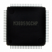
M38D59GCHP#U0 Renesas Electronics America, M38D59GCHP#U0 Datasheet - Page 131

M38D59GCHP#U0
Manufacturer Part Number
M38D59GCHP#U0
Description
IC 740/38D5 MCU QZ-ROM 80LQFP
Manufacturer
Renesas Electronics America
Series
740/38000r
Datasheet
1.M38D58G8FPU0.pdf
(144 pages)
Specifications of M38D59GCHP#U0
Core Processor
740
Core Size
8-Bit
Speed
12.5MHz
Connectivity
SIO, UART/USART
Peripherals
LCD, LED, PWM, WDT
Number Of I /o
59
Program Memory Size
48KB (48K x 8)
Program Memory Type
QzROM
Ram Size
2K x 8
Voltage - Supply (vcc/vdd)
1.8 V ~ 5.5 V
Data Converters
A/D 8x10b
Oscillator Type
Internal
Operating Temperature
-20°C ~ 85°C
Package / Case
80-LQFP
Lead Free Status / RoHS Status
Lead free / RoHS Compliant
Eeprom Size
-
Available stocks
Company
Part Number
Manufacturer
Quantity
Price
38D5 Group
Rev.3.04
REJ03B0158-0304
Notes on A/D Conversion
1. Analog Input Pin
Set the signal source impedance for analog input low, or equip an
analog input pin with an external capacitor of 0.01 µ F to 1 µ F.
In addition, operations of application products should be verified
thoroughly on the user side.
<Reason>
An analog input pin has a built-in capacitor for analog voltage
comparison. Thus if a signal from the high impedance signal
source is input to the analog input pin, charge and discharge
n o i s e w i l l b e g e n e r a t e d . T h i s m a y c a u s e t h e A / D
conversion/comparison accuracy to drop.
2. Clock Frequency during A/D Conversion
The comparator input consists of a capacity coupling. If the
conversion rate is too low, the A/D conversion accuracy may
deteriorate due to a charge lost, so set f(X
A/D conversion in X
WIT instruction during A/D conversion.
In low-speed mode (when on-chip oscillator is selected), as A/D
conversion is performed using the internal on-chip oscillator,
there is no limit on the minimum frequency for f(X
3. ADKEY Function
When the ADKEY enable bit is set to “1”, the analog input pin
selection bits are disabled. Do not execute the A/D conversion by
a program while ADKEY is enabled. Enabling ADKEY does not
change bits 0 to 2 of ADCON.
4. A/D Conversion Immediately After ADKEY Function
In the ADKEY function, A/D conversion is not performed to the
analog input voltage immediately after starting the function. This
causes the A/D conversion result immediately after starting the
function to be undefined. If the A/D conversion result of the
analog input voltage applied to the ADKEY pin is required,
select the analog input pin corresponding to ADKEY before
performing A/D conversion.
5. Input Voltage Applied to ADKEY Pin
Set the input to the ADKEY pin into a steep falling waveform
and stabilize the input voltage within eight cycles (1 µ s when
f(X
or lower.
The actual threshold voltage for the ADKEY pin is between V
and V
To prevent unnecessary ADKEY operation due to noise or other
factors, set the ADKEY pin voltage to V
while the input is waited.
IN
Started
) = 8 MHz) from the moment the input voltage reaches V
IL
.
May 20, 2008 Page 129 of 134
IN
mode. Also, do not execute the STP or
IN
IH
) 500 kHz or more for
(0.9 V
IN
CC
).
) or more
IH
IL
6. Register Operation during A/D Conversion
The A/D conversion operation is not guaranteed if the following
are preformed:
• The CPU mode register is operated during A/D conversion
• The AD control register is operated during A/D conversion
• The STP or WIT instruction is executed during A/D
7. A/D Converter Power Source Pin
Connect to the A/D converter power source pin to AV
whether the A/D conversion function is used or not.
<Reason>
If the AV
because the pin will be affected by noise or other factors.
operation
operation
conversion operation
SS
pin is left open, the MCU may operate incorrectly
SS
or V
SS


