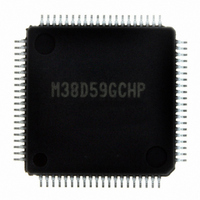
M38D59GCHP#U0 Renesas Electronics America, M38D59GCHP#U0 Datasheet - Page 132

M38D59GCHP#U0
Manufacturer Part Number
M38D59GCHP#U0
Description
IC 740/38D5 MCU QZ-ROM 80LQFP
Manufacturer
Renesas Electronics America
Series
740/38000r
Datasheet
1.M38D58G8FPU0.pdf
(144 pages)
Specifications of M38D59GCHP#U0
Core Processor
740
Core Size
8-Bit
Speed
12.5MHz
Connectivity
SIO, UART/USART
Peripherals
LCD, LED, PWM, WDT
Number Of I /o
59
Program Memory Size
48KB (48K x 8)
Program Memory Type
QzROM
Ram Size
2K x 8
Voltage - Supply (vcc/vdd)
1.8 V ~ 5.5 V
Data Converters
A/D 8x10b
Oscillator Type
Internal
Operating Temperature
-20°C ~ 85°C
Package / Case
80-LQFP
Lead Free Status / RoHS Status
Lead free / RoHS Compliant
Eeprom Size
-
Available stocks
Company
Part Number
Manufacturer
Quantity
Price
- Current page: 132 of 144
- Download datasheet (3Mb)
38D5 Group
Rev.3.04
REJ03B0158-0304
Notes on LCD Drive Control Circuit
1. Multiplier Circuit
When the multiplier circuit is used, set the multiplier circuit
control bit to “1” (multiplier circuit enabled) after applying a
voltage from 1.3 V or more to 2.1 V or less to the V
When the multiplier circuit is not used, set the V
to “1” (open) and apply an appropriate voltage to the LCD power
source input pins (V
set open, the V
When the multiplier circuit is used, set the LCDCK frequency to
100 Hz or more. The on-chip oscillator cannot be used as
LCDCK.
In a system where the multiplier circuit is used (a multiplier
capacitor is externally connected between the C
set the multiplier circuit control bit to “1” (multiplier circuit
enabled) before executing the STP or WIT instruction.
Fig. 105 Processing example when writing data to LCD display RAM While LCD Turned On
(1) Correct processing
May 20, 2008 Page 130 of 134
(2) Incorrect processing
L3
LCD
on
LCD
on or
off
LCD
on
LCD
off
LCD
on or
off
pin is placed in the high impedance state.
L1
to V
L3
). When the V
Set LCD display RAM data
LRAM0 (address 0840
Set LCD display RAM data
LRAM0 (address 0840
Set LCD display RAM data
LRAM0 (address 0840
LCD on or off?
LCD on or off?
L3
On
*Content at address 0840
On
*Content at address 0840
L3
connection bit is
16
16
16
1
) ← “FF
) ← “FF
) ← “00
connection bit
and C
L1
pin.
16
16
16
Off
Off
”
”
”
2
pins),
16
: “FF
16
Set LCD display RAM data
LRAM0 (address 0840
: “FF
2. Setting Data to LCD Display RAM
To write data to the LCD display RAM when the LCD enable bit
is set to “1” and while LCD is turned on, set fixed data.
Rewriting with temporary data may cause LCD to flicker. The
following shows a processing example to write data to the LCD
display RAM while LCD is turned on.
16
”
• Set off data to LCD display RAM
• Set fixed data to LCD display RAM
16
”
16
) ←“00
16
”
• Set fixed data to LCD display RAM
Related parts for M38D59GCHP#U0
Image
Part Number
Description
Manufacturer
Datasheet
Request
R

Part Number:
Description:
KIT STARTER FOR M16C/29
Manufacturer:
Renesas Electronics America
Datasheet:

Part Number:
Description:
KIT STARTER FOR R8C/2D
Manufacturer:
Renesas Electronics America
Datasheet:

Part Number:
Description:
R0K33062P STARTER KIT
Manufacturer:
Renesas Electronics America
Datasheet:

Part Number:
Description:
KIT STARTER FOR R8C/23 E8A
Manufacturer:
Renesas Electronics America
Datasheet:

Part Number:
Description:
KIT STARTER FOR R8C/25
Manufacturer:
Renesas Electronics America
Datasheet:

Part Number:
Description:
KIT STARTER H8S2456 SHARPE DSPLY
Manufacturer:
Renesas Electronics America
Datasheet:

Part Number:
Description:
KIT STARTER FOR R8C38C
Manufacturer:
Renesas Electronics America
Datasheet:

Part Number:
Description:
KIT STARTER FOR R8C35C
Manufacturer:
Renesas Electronics America
Datasheet:

Part Number:
Description:
KIT STARTER FOR R8CL3AC+LCD APPS
Manufacturer:
Renesas Electronics America
Datasheet:

Part Number:
Description:
KIT STARTER FOR RX610
Manufacturer:
Renesas Electronics America
Datasheet:

Part Number:
Description:
KIT STARTER FOR R32C/118
Manufacturer:
Renesas Electronics America
Datasheet:

Part Number:
Description:
KIT DEV RSK-R8C/26-29
Manufacturer:
Renesas Electronics America
Datasheet:

Part Number:
Description:
KIT STARTER FOR SH7124
Manufacturer:
Renesas Electronics America
Datasheet:

Part Number:
Description:
KIT STARTER FOR H8SX/1622
Manufacturer:
Renesas Electronics America
Datasheet:

Part Number:
Description:
KIT DEV FOR SH7203
Manufacturer:
Renesas Electronics America
Datasheet:


