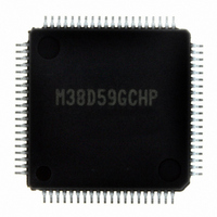
M38D59GCHP#U0 Renesas Electronics America, M38D59GCHP#U0 Datasheet - Page 37

M38D59GCHP#U0
Manufacturer Part Number
M38D59GCHP#U0
Description
IC 740/38D5 MCU QZ-ROM 80LQFP
Manufacturer
Renesas Electronics America
Series
740/38000r
Datasheet
1.M38D58G8FPU0.pdf
(144 pages)
Specifications of M38D59GCHP#U0
Core Processor
740
Core Size
8-Bit
Speed
12.5MHz
Connectivity
SIO, UART/USART
Peripherals
LCD, LED, PWM, WDT
Number Of I /o
59
Program Memory Size
48KB (48K x 8)
Program Memory Type
QzROM
Ram Size
2K x 8
Voltage - Supply (vcc/vdd)
1.8 V ~ 5.5 V
Data Converters
A/D 8x10b
Oscillator Type
Internal
Operating Temperature
-20°C ~ 85°C
Package / Case
80-LQFP
Lead Free Status / RoHS Status
Lead free / RoHS Compliant
Eeprom Size
-
Available stocks
Company
Part Number
Manufacturer
Quantity
Price
38D5 Group
Rev.3.04
REJ03B0158-0304
TIMERS
8-Bit Timer
The 38D5 Group has four built-in 8-bit timers: Timer 1, Timer 2,
Timer 3, and Timer 4.
Fig. 25 Timer 1-4 block diagram
P7
P7
T
P7
T
2
4OUT
3OUT
/T
4
The following values can be selected
the clock for Timer;
1/1, 1/2, 1/16, 1/256
3
/PWM
2OUT
/PWM
φ SOURCE
P7
register
2
P7
register
Timer 4 output selection bit
direction
P7
register
/CKOUT
Timer 3 output selection bit
3
1
0
4
direction
/
May 20, 2008 Page 35 of 134
/
direction
(1)
Timer 2 output selection bit
Timer 3 operating
mode selection bit
P7
Timer 4 operating
mode selection bit
Frequency divider
2
clock output control bit
P7
latch
2
P7
latch
P7
latch
“01”
“00”
“10”
3
4
“1”
“0”
T
edge switch bit
“0”
“1”
T
edge switch bit
3OUT
4OUT
X
System
clock φ
Timer 3 output selection bit
Timer 4 output selection bit
CIN
T
edge switch bit
output
Note1: φSOURCE indicates the followings:
2OUT
output
Clock for
Timer 3
“0”
“1”
Clock for
Timer 4
“0”
“1”
Clock for
Timer 2
Clock for
Timer 1
Timer Y
output
output
10 bit
PWM0
circuit
10 bit
PWM1
circuit
Q
Q
Q
Q
•X
•On-chip oscillator divided by 4 in the on-chip oscillator mode
•Sub-clock in the low-speed mode
S
S
“0”
“1”
T
T
IN
1/2
1/2
Timer 2 output selection bit
Q
Q
input in the frequency/2, 4, or 8 mode
S
8
T
X
CIN
1/2
f(X
IN
Timer 1
Timer 2
Timer 3
Timer 4
)
“01”
“10”
“1”
“00”
“01”
“01”
“00”
“0”
“10”
“10”
“00”
Timer 3 count source
selection bit
Timer 4 count source
selection bits
“11”
Timer 2 count
source selection
bits
Timer 1 count
source selection
bits
Frequency division
selection bits
(2 bits for each Timer)
Timer 2 count stop bit
Timer 3 count stop bit
Timer 1 count stop bit
Timer 4 count stop bit
Each timer has the 8-bit timer latch. All timers are down-
counters.
When the timer reaches “00
reloaded into the timer with the next count pulse. In this mode,
the interrupt request bit corresponding to that timer is set to “1”.
The count can be stopped by setting the stop bit of each timer to
“1”.
PWM01 register (2)
PWM01 register (2)
Timer 4 latch (8)
Timer 1 latch (8)
Timer 2 latch (8)
Timer 3 latch (8)
Timer 1 (8)
Timer 2 (8)
Timer 3 (8)
Timer 4 (8)
Data bus
16
”, the contents of the timer latch is
Timer 3 write control bit
Timer 2 write control bit
Timer 4 write control bit
Timer 1 interrupt request
Timer 2 interrupt request
Timer 3 interrupt request
Timer 4 interrupt request


