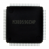
M38D59GCHP#U0 Renesas Electronics America, M38D59GCHP#U0 Datasheet - Page 62

M38D59GCHP#U0
Manufacturer Part Number
M38D59GCHP#U0
Description
IC 740/38D5 MCU QZ-ROM 80LQFP
Manufacturer
Renesas Electronics America
Series
740/38000r
Datasheet
1.M38D58G8FPU0.pdf
(144 pages)
Specifications of M38D59GCHP#U0
Core Processor
740
Core Size
8-Bit
Speed
12.5MHz
Connectivity
SIO, UART/USART
Peripherals
LCD, LED, PWM, WDT
Number Of I /o
59
Program Memory Size
48KB (48K x 8)
Program Memory Type
QzROM
Ram Size
2K x 8
Voltage - Supply (vcc/vdd)
1.8 V ~ 5.5 V
Data Converters
A/D 8x10b
Oscillator Type
Internal
Operating Temperature
-20°C ~ 85°C
Package / Case
80-LQFP
Lead Free Status / RoHS Status
Lead free / RoHS Compliant
Eeprom Size
-
Available stocks
Company
Part Number
Manufacturer
Quantity
Price
- Current page: 62 of 144
- Download datasheet (3Mb)
38D5 Group
Rev.3.04
REJ03B0158-0304
CLOCK OUTPUT FUNCTION
A system clock φ can be output from I/O port P7
function of I/O port, timer 2 output function and system clock φ
output function are controlled by the clock output control register
(address 0FF3
12 mode register (address 0025
In order to output a system clock φ from I/O port P7
timer 2 output selection bit to “1” and P7
bits of the clock output control register to “01”. In order to output
the same signal as oscillation frequency of sub clock X
the P7
function is selected, a clock is output while the direction register
of port P7
P7
the clock output) except port at the cycle after the timer 2 output
selection bit is switched.
Fig. 55 Block diagram of Clock output function
Other function registers
[RRF register (RRFR)]
The RRF register (address 0012
not have the control function.
As for the value written in this register, high-order 4 bits and
low-order 4 bits interchange.
It is initialized after reset.
2
is switched to the port output or the output (timer 2 output or
2
clock output control bits to “10”. When the clock output
Timer 2 latch (8)
2
Timer 2 (8)
is set to the output mode.
May 20, 2008 Page 60 of 134
16
) and the timer 2 output selection bit of the timer
Timer 2 output selection bit
16
16
).
) is the 8-bit register and does
1/2
T
System clock φ
S
Q
Q
2
clock output control
“0”
“1”
T
switch bit
2OUT
X
2
CIN
. The triple
P7
control bits
output edge
2
2
, set the
CIN
“00”
“01”
clock output
“10”
, set
Fig. 54 Structure of clock output control register
Fig. 56 Structure of RRF register
b7
b7
b7
P7
2
latch
b0
Timer 2 output selection bit
Timer 12 mode register (address 0025
T12M
Timer 2 output selection bit
b0
0 : I/O port
1 : Timer 2 output
Clock output control register
(CKOUT : address 0FF3
P7
Not used (returns “0” when read)
b1b0
0 0: Timer 2 output
0 1: φ frequency signal output
1 0: X
1 1: Not available
2
clock output control bits
P7
b0
CIN
2
direction register
frequency signal output
RRF register
(RRFR : address 0012
DB
DB
DB
DB
DB
DB
DB
DB
4
5
6
7
0
1
2
3
data storage
data storage
data storage
data storage
data storage
data storage
data storage
data storage
P7
2
16
/T
)
2
OUT/CKOUT
16
)
16
)
Related parts for M38D59GCHP#U0
Image
Part Number
Description
Manufacturer
Datasheet
Request
R

Part Number:
Description:
KIT STARTER FOR M16C/29
Manufacturer:
Renesas Electronics America
Datasheet:

Part Number:
Description:
KIT STARTER FOR R8C/2D
Manufacturer:
Renesas Electronics America
Datasheet:

Part Number:
Description:
R0K33062P STARTER KIT
Manufacturer:
Renesas Electronics America
Datasheet:

Part Number:
Description:
KIT STARTER FOR R8C/23 E8A
Manufacturer:
Renesas Electronics America
Datasheet:

Part Number:
Description:
KIT STARTER FOR R8C/25
Manufacturer:
Renesas Electronics America
Datasheet:

Part Number:
Description:
KIT STARTER H8S2456 SHARPE DSPLY
Manufacturer:
Renesas Electronics America
Datasheet:

Part Number:
Description:
KIT STARTER FOR R8C38C
Manufacturer:
Renesas Electronics America
Datasheet:

Part Number:
Description:
KIT STARTER FOR R8C35C
Manufacturer:
Renesas Electronics America
Datasheet:

Part Number:
Description:
KIT STARTER FOR R8CL3AC+LCD APPS
Manufacturer:
Renesas Electronics America
Datasheet:

Part Number:
Description:
KIT STARTER FOR RX610
Manufacturer:
Renesas Electronics America
Datasheet:

Part Number:
Description:
KIT STARTER FOR R32C/118
Manufacturer:
Renesas Electronics America
Datasheet:

Part Number:
Description:
KIT DEV RSK-R8C/26-29
Manufacturer:
Renesas Electronics America
Datasheet:

Part Number:
Description:
KIT STARTER FOR SH7124
Manufacturer:
Renesas Electronics America
Datasheet:

Part Number:
Description:
KIT STARTER FOR H8SX/1622
Manufacturer:
Renesas Electronics America
Datasheet:

Part Number:
Description:
KIT DEV FOR SH7203
Manufacturer:
Renesas Electronics America
Datasheet:


