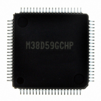
M38D59GCHP#U0 Renesas Electronics America, M38D59GCHP#U0 Datasheet - Page 53

M38D59GCHP#U0
Manufacturer Part Number
M38D59GCHP#U0
Description
IC 740/38D5 MCU QZ-ROM 80LQFP
Manufacturer
Renesas Electronics America
Series
740/38000r
Datasheet
1.M38D58G8FPU0.pdf
(144 pages)
Specifications of M38D59GCHP#U0
Core Processor
740
Core Size
8-Bit
Speed
12.5MHz
Connectivity
SIO, UART/USART
Peripherals
LCD, LED, PWM, WDT
Number Of I /o
59
Program Memory Size
48KB (48K x 8)
Program Memory Type
QzROM
Ram Size
2K x 8
Voltage - Supply (vcc/vdd)
1.8 V ~ 5.5 V
Data Converters
A/D 8x10b
Oscillator Type
Internal
Operating Temperature
-20°C ~ 85°C
Package / Case
80-LQFP
Lead Free Status / RoHS Status
Lead free / RoHS Compliant
Eeprom Size
-
Available stocks
Company
Part Number
Manufacturer
Quantity
Price
38D5 Group
Rev.3.04
REJ03B0158-0304
Fig. 42 Structure of AD control register
At 10bitAD
(Read address 0017
At 8bitAD
(Read only address 0017
AD conversion register
high-order
(Address 0017
AD conversion register
low-order
(Address 0016
(Address 0017
* V
Note : The bit 5 to bit 1 of address 0016
Notes 1: φSOURCE indicates the followings:
0: ON only during A/D conversion
1: ON
REF
b7
input switch bit
Also, bit 0 is undefined at reading.
2: When the ADKEY enable bit is “1”, the analog input pin selection
bits are invalid.
Do not execute the A/D conversion by program while the ADKEY is
enabled.
Bit 0 to bit 2 of ADCON are not changed even when ADKEY is
enabled.
•X
•On-chip oscillator divided by 4 in the low-speed and the on-chip
oscillator mode
May 20, 2008 Page 51 of 134
16
16
16
IN
)
)
)
input in the frequency/2, 4, or 8 mode
16
before 0016
16
)
b0
16
AD control register
(ADCON: address 0015
)
b7
b7
Analog input pin selection bits
b2 b1 b0
0 0 0 : P5
0 0 1 : P5
0 1 0 : P5
0 1 1 : P5
1 0 0 : P5
1 0 1 : P5
1 1 0 : P5
1 1 1 : P5
AD conversion completion bit
AD conversion clock selection bit
ADKEY enable bit
10-bit or 8-bit conversion switch bit
ADKEY selection bit
b7
b9 b8
b1 b0
b7 b6
0 : Conversion in progress
1 : Conversion completed
0 : φSOURCE/2
1 : φSOURCE/8
0 : Disabled
1 : Enabled
0 : 10-bit AD
1 : 8-bit AD
0 : Invalid
1 : Valid
16
become “0” at reading.
b7
b5
0
1
2
3
4
5
6
7
b4 b3 b2
b6 b5 b4
/AN
/AN
/AN
/AN
/AN
/AN
/AN
/AN
0
1
2
3
4
5
6
7
(1)
( 2 )
b1
16
b3
)
b0
b0
b2
b0
b0
*
(high-order)
(low-order)
ADKEY function
The ADKEY function is used to judge the analog input voltage
input from the ADKEY pin. When the A/D converter starts
operating after V
analog voltage input can be judged with the A/D conversion
interrupt.
This function can be used with the STP and WIT state.
As for the ADKEY function in 38D5 Group, the A/D conversion
of analog input voltage immediately after starting ADKEY
function is not performed.
Therefore, the A/D conversion result immediately after an
ADKEY function is undefined. Accordingly, when the A/D
conversion result of the analog input voltage input from the
ADKEY pin is required, start the A/D conversion by program
after the analog input pin corresponding to ADKEY is selected.
• ADKEY Selection
When the ADKEY pin is used, set the ADKEY selection bit to
“1”. The ADKEY selection bit is “0”, just after the A/D
conversion is started.
• ADKEY Enable
The ADKEY function is enabled by writing “1” to the ADKEY
enable bit. Surely, in order to enable ADKEY function, set “1” to
the ADKEY enable bit, after setting the ADKEY selection bit to
“1”.
When the ADKEY enable bit of the AD control register is “1”,
the analog input pin selection bits become invalid. Please do not
write “0” in the AD conversion completion bit by the program
during ADKEY enabled state.
[ADKEY Control Circuit]
In order to obtain a more exact conversion result, by the A/D
conversion with ADKEY, execute the following;
• set the input to the ADKEY pin into a steep falling waveform,
• stabilize the input voltage within 8 clock cycles (1 µs at f(X
The threshold voltage with an actual ADKEY pin is the voltage
between V
In order not to make ADKEY operation perform superfluously in
a noise etc., in the state of the waiting for an input, set the voltage
of an ADKEY pin to V
When the following operations are performed, the A/D
conversion operation cannot be guaranteed.
• When the CPU mode register is operated during A/D
• When the AD conversion control register is operated during
• When the STP or WIT instruction is executed during A/D
= 8 MHz) after the input voltage is under V
conversion operation,
A/D conversion operation,
conversion operation.
IH
-V
IL
.
IL
(0.7 × Vcc-0.5) or less is input, the event of
IH
(0.9V
CC
) or more.
IL
IN
)


