DF2505FC26V Renesas Electronics America, DF2505FC26V Datasheet - Page 46
DF2505FC26V
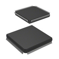
Manufacturer Part Number
DF2505FC26V
Description
IC H8S/2505 MCU FLASH 144QFP
Manufacturer
Renesas Electronics America
Series
H8® H8S/2500r
Specifications of DF2505FC26V
Core Processor
H8S/2000
Core Size
16-Bit
Speed
26MHz
Connectivity
I²C, SCI
Peripherals
POR, PWM, WDT
Number Of I /o
104
Program Memory Size
384KB (384K x 8)
Program Memory Type
FLASH
Ram Size
32K x 8
Voltage - Supply (vcc/vdd)
3 V ~ 5.5 V
Data Converters
A/D 16x10b; D/A 2x8b
Oscillator Type
Internal
Operating Temperature
-40°C ~ 85°C
Package / Case
144-QFP
Lead Free Status / RoHS Status
Lead free / RoHS Compliant
Eeprom Size
-


Section 13 Serial Communication Interface (SCI)
Table 13.1
Table 13.2
Table 13.3
Table 13.4
Table 13.5
Table 13.6
Table 13.7
Table 13.8
Table 13.9
Table 13.10 Serial Transfer Formats (Asynchronous Mode) ...................................................... 426
Table 13.11 SSR Status Flags and Receive Data Handling ........................................................ 433
Table 13.12 Interrupt Sources of Serial Communication Interface Mode................................... 465
Table 13.13 Interrupt Sources in Smart Card Interface Mode .................................................... 466
Section 14 I
Table 14.1
Table 14.2
Table 14.3
Table 14.4
Section 15 A/D Converter
Table 15.1
Table 15.2
Table 15.3
Table 15.4
Table 15.5
Table 15.6
Section 16 D/A Converter
Table 16.1
Table 16.2
Section 17 IEBus™ Controller (IEB) [H8S/2552 Group]
Table 17.1
Table 17.2
Table 17.3
Rev. 6.00 Sep. 24, 2009 Page xliv of xlvi
REJ09B0099-0600
Pin Configuration .................................................................................................... 397
Relationships between N Setting in BRR and Bit Rate B ....................................... 418
BRR Settings for Various Bit Rates (Asynchronous Mode) ................................... 419
Maximum Bit Rate for Each Frequency (Asynchronous Mode)............................. 420
Maximum Bit Rate with External Clock Input (Asynchronous Mode)................... 421
BRR Settings for Various Bit Rates (Clocked Synchronous Mode) ....................... 422
Maximum Bit Rate with External Clock Input (Clocked Synchronous Mode)....... 423
Examples of Bit Rate for Various BRR Settings (Smart Card Interface Mode)
(When n = 0 and S = 372) ....................................................................................... 423
Maximum Bit Rate at Various Frequencies (Smart Card Interface Mode)
(when S = 372)........................................................................................................ 424
I
Transfer Rate........................................................................................................... 481
Interrupt Requests ................................................................................................... 509
Time for Monitoring SCL ....................................................................................... 510
Pin Configuration .................................................................................................... 515
Analog Input Channels and Corresponding ADDR Registers ................................ 516
A/D Conversion Time (Single Mode) ..................................................................... 525
A/D Conversion Time (Scan Mode) ....................................................................... 526
A/D Converter Interrupt Source .............................................................................. 527
Analog Pin Specifications ....................................................................................... 531
Pin Configuration .................................................................................................... 534
D/A Conversion Control ......................................................................................... 536
Mode Types............................................................................................................. 541
Transfer speed and Maximum Number of Transfer Bytes in Each Communications
Mode ....................................................................................................................... 542
Contents of Message Length bits ............................................................................ 547
2
2
C Bus Interface 2 (IIC2)
C Bus Interface Pins ............................................................................................. 478
Related parts for DF2505FC26V
Image
Part Number
Description
Manufacturer
Datasheet
Request
R

Part Number:
Description:
KIT STARTER FOR M16C/29
Manufacturer:
Renesas Electronics America
Datasheet:

Part Number:
Description:
KIT STARTER FOR R8C/2D
Manufacturer:
Renesas Electronics America
Datasheet:

Part Number:
Description:
R0K33062P STARTER KIT
Manufacturer:
Renesas Electronics America
Datasheet:

Part Number:
Description:
KIT STARTER FOR R8C/23 E8A
Manufacturer:
Renesas Electronics America
Datasheet:

Part Number:
Description:
KIT STARTER FOR R8C/25
Manufacturer:
Renesas Electronics America
Datasheet:

Part Number:
Description:
KIT STARTER H8S2456 SHARPE DSPLY
Manufacturer:
Renesas Electronics America
Datasheet:

Part Number:
Description:
KIT STARTER FOR R8C38C
Manufacturer:
Renesas Electronics America
Datasheet:

Part Number:
Description:
KIT STARTER FOR R8C35C
Manufacturer:
Renesas Electronics America
Datasheet:

Part Number:
Description:
KIT STARTER FOR R8CL3AC+LCD APPS
Manufacturer:
Renesas Electronics America
Datasheet:
Part Number:
Description:
KIT STARTER FOR RX610
Manufacturer:
Renesas Electronics America
Datasheet:

Part Number:
Description:
KIT STARTER FOR R32C/118
Manufacturer:
Renesas Electronics America
Datasheet:

Part Number:
Description:
KIT DEV RSK-R8C/26-29
Manufacturer:
Renesas Electronics America
Datasheet:

Part Number:
Description:
KIT STARTER FOR SH7124
Manufacturer:
Renesas Electronics America
Datasheet:

Part Number:
Description:
KIT STARTER FOR H8SX/1622
Manufacturer:
Renesas Electronics America
Datasheet:

Part Number:
Description:
KIT DEV FOR SH7203
Manufacturer:
Renesas Electronics America
Datasheet: