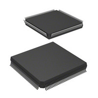
DF2505FC26V Renesas Electronics America, DF2505FC26V Datasheet - Page 854

DF2505FC26V
Manufacturer Part Number
DF2505FC26V
Description
IC H8S/2505 MCU FLASH 144QFP
Manufacturer
Renesas Electronics America
Series
H8® H8S/2500r
Specifications of DF2505FC26V
Core Processor
H8S/2000
Core Size
16-Bit
Speed
26MHz
Connectivity
I²C, SCI
Peripherals
POR, PWM, WDT
Number Of I /o
104
Program Memory Size
384KB (384K x 8)
Program Memory Type
FLASH
Ram Size
32K x 8
Voltage - Supply (vcc/vdd)
3 V ~ 5.5 V
Data Converters
A/D 16x10b; D/A 2x8b
Oscillator Type
Internal
Operating Temperature
-40°C ~ 85°C
Package / Case
144-QFP
Lead Free Status / RoHS Status
Lead free / RoHS Compliant
Eeprom Size
-
- Current page: 854 of 980
- Download datasheet (6Mb)
Section 22 Power-Down Modes
22.7
22.7.1
CPU operation makes a transition to watch mode when the SLEEP instruction is executed in high-
speed mode with SSBY bit in SBYCR = 1, DTON bit in LPWRCR = 0, and PSS bit in TCSR_1
(WDT_1) = 1.
In watch mode, the CPU is stopped and peripheral modules other than the WDT_1 are also
stopped. The contents of the CPU's internal registers, the data in on-chip RAM, and the statuses of
the internal peripheral modules (excluding the HCAN*
functions) and I/O ports are retained. To make a transition to watch mode, bits SCK2 to SCK0 in
SCKCR must be set to 0.
Notes: 1. Supported only by the H8S/2556 Group.
22.7.2
Watch mode is cleared by any interrupt (WOVI1 interrupt, NMI pin, or IRQ0 to IRQ7), or signals
at the RES, MRES, or STBY pin.
• Clearing with an interrupt
• Clearing with the RES pin or MRES pin
• Clearing with the STBY pin
Rev. 6.00 Sep. 24, 2009 Page 806 of 928
REJ09B0099-0600
When an interrupt occurs, watch mode is cleared and a transition is made to high-speed mode
or medium-speed mode. When a transition is made to high-speed mode, a stable clock is
supplied to all LSI circuits and interrupt exception processing starts after the time set in the
STS2 to STS0 bits in SBYCR has elapsed. In the case of IRQ0 to IRQ7 interrupts, no
transition is made from watch mode if the corresponding enable bit/pin function switching bit
has been cleared to 0, and, in the case of interrupts from the internal peripheral modules, the
interrupt enable register has been set to disable the reception of that interrupt, or is masked by
the CPU.
See section 22.4.3, Oscillation Settling Time after Clearing Software Standby Mode, for how
to set the oscillation settling time when making a transition from watch mode to high-speed
mode.
For clearing watch mode by the RES pin or MRES pin, see section 22.4.2, Clearing Software
Standby Mode.
When the STBY pin is driven low, a transition is made to hardware standby mode.
2. Supported only by the H8S/2552 Group.
Watch Mode
Transition to Watch Mode
Clearing Watch Mode
1
, IEB*
2
, A/D converter, and some IIC2
Related parts for DF2505FC26V
Image
Part Number
Description
Manufacturer
Datasheet
Request
R

Part Number:
Description:
KIT STARTER FOR M16C/29
Manufacturer:
Renesas Electronics America
Datasheet:

Part Number:
Description:
KIT STARTER FOR R8C/2D
Manufacturer:
Renesas Electronics America
Datasheet:

Part Number:
Description:
R0K33062P STARTER KIT
Manufacturer:
Renesas Electronics America
Datasheet:

Part Number:
Description:
KIT STARTER FOR R8C/23 E8A
Manufacturer:
Renesas Electronics America
Datasheet:

Part Number:
Description:
KIT STARTER FOR R8C/25
Manufacturer:
Renesas Electronics America
Datasheet:

Part Number:
Description:
KIT STARTER H8S2456 SHARPE DSPLY
Manufacturer:
Renesas Electronics America
Datasheet:

Part Number:
Description:
KIT STARTER FOR R8C38C
Manufacturer:
Renesas Electronics America
Datasheet:

Part Number:
Description:
KIT STARTER FOR R8C35C
Manufacturer:
Renesas Electronics America
Datasheet:

Part Number:
Description:
KIT STARTER FOR R8CL3AC+LCD APPS
Manufacturer:
Renesas Electronics America
Datasheet:

Part Number:
Description:
KIT STARTER FOR RX610
Manufacturer:
Renesas Electronics America
Datasheet:

Part Number:
Description:
KIT STARTER FOR R32C/118
Manufacturer:
Renesas Electronics America
Datasheet:

Part Number:
Description:
KIT DEV RSK-R8C/26-29
Manufacturer:
Renesas Electronics America
Datasheet:

Part Number:
Description:
KIT STARTER FOR SH7124
Manufacturer:
Renesas Electronics America
Datasheet:

Part Number:
Description:
KIT STARTER FOR H8SX/1622
Manufacturer:
Renesas Electronics America
Datasheet:

Part Number:
Description:
KIT DEV FOR SH7203
Manufacturer:
Renesas Electronics America
Datasheet:


