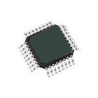
MC68HC908EY16CFA Freescale Semiconductor, MC68HC908EY16CFA Datasheet - Page 112

MC68HC908EY16CFA
Manufacturer Part Number
MC68HC908EY16CFA
Description
IC MCU 16K FLASH 8MHZ SPI 32LQFP
Manufacturer
Freescale Semiconductor
Series
HC08r
Datasheet
1.MC908EY16VFAR2.pdf
(278 pages)
Specifications of MC68HC908EY16CFA
Core Processor
HC08
Core Size
8-Bit
Speed
8MHz
Connectivity
LIN, SCI, SPI
Peripherals
POR, PWM
Number Of I /o
24
Program Memory Size
16KB (16K x 8)
Program Memory Type
FLASH
Ram Size
512 x 8
Voltage - Supply (vcc/vdd)
4.5 V ~ 5.5 V
Data Converters
A/D 8x10b
Oscillator Type
Internal
Operating Temperature
-40°C ~ 85°C
Package / Case
32-LQFP
Processor Series
HC08EY
Core
HC08
Data Bus Width
8 bit
Data Ram Size
512 B
Interface Type
ESCI, SPI
Maximum Clock Frequency
8 MHz
Number Of Programmable I/os
24
Number Of Timers
4
Maximum Operating Temperature
+ 85 C
Mounting Style
SMD/SMT
Development Tools By Supplier
FSICEBASE, M68CBL05CE, ZK-HC08EY-A
Minimum Operating Temperature
- 40 C
On-chip Adc
10 bit, 8 Channel
Lead Free Status / RoHS Status
Contains lead / RoHS non-compliant
Eeprom Size
-
Lead Free Status / Rohs Status
No
Available stocks
Company
Part Number
Manufacturer
Quantity
Price
Company:
Part Number:
MC68HC908EY16CFA
Manufacturer:
FREESCALE
Quantity:
1 831
Company:
Part Number:
MC68HC908EY16CFA
Manufacturer:
QFP
Quantity:
453
Company:
Part Number:
MC68HC908EY16CFA
Manufacturer:
Freescale Semiconductor
Quantity:
10 000
- Current page: 112 of 278
- Download datasheet (2Mb)
Low-Voltage Inhibit (LVI) Module
Once an LVI reset occurs, the MCU remains in reset until V
be above LVI
Operation). The output of the comparator controls the state of the LVIOUT flag in the LVI status register
(LVISR).
An LVI reset also drives the RST pin low to provide low-voltage protection to external peripheral devices.
11.3.1 Polled LVI Operation
In applications that can operate at V
polling the LVIOUT bit. In the configuration register, the LVIPWRD bit must be at 0 to enable the LVI
module, and the LVIRSTD bit must be at 1 to disable LVI resets.
11.3.2 Forced Reset Operation
In applications that require V
module to reset the MCU when V
and LVIRSTD bits must be at 0 to enable the LVI module and to enable LVI resets.
11.3.3 False Reset Protection
False reset protection is provided by the hysteresis in the LVI trip circuit (refer to
to
11.3.4 LVI Status Register
The LVI status register flags V
LVIOUT — LVI Output Bit
112
20.5 DC Electrical Characteristics
This read-only flag becomes set when the V
Table
11-1.) Reset clears the LVIOUT bit.
TRIPR
Address:
Reset:
Read:
Write:
for only one CPU cycle to bring the MCU out of reset (see
LVIOUT
$FE0C
At Level:
Bit 7
0
MC68HC908EY16 • MC68HC908EY8 Data Sheet, Rev. 10
DD
DD
Figure 11-2. LVI Status Register (LVISR)
= Unimplemented
LVI
to remain above the LVI
DD
TRIPF
voltages below the LVI
6
0
0
Table 11-1. LVIOUT Bit Indication
V
V
falls to the LVI
DD
DD
DD
for hysteresis value (VHYS) and rising and falling LVI trip values.
< V
> LVI
< LVI
levels below the LVI
V
DD
DD
5
0
0
TRIPR
TRIPF
< LVI
DD
TRIPR
TRIPF
voltage falls below the LVI
4
0
0
level. In the configuration register, the LVIPWRD
TRIPF
TRIPF
DD
TRIPF
3
0
0
rises above a voltage, LVI
level, enabling LVI resets allows the LVI
level
Previous Value
level, software can monitor V
.
LVIOUT
2
0
0
0
1
TRIPF
11.3.2 Forced Reset
Table
1
0
0
voltage. (See
Freescale Semiconductor
11-1). Please refer
Bit 0
TRIPR
0
0
. V
DD
DD
by
must
Related parts for MC68HC908EY16CFA
Image
Part Number
Description
Manufacturer
Datasheet
Request
R
Part Number:
Description:
Manufacturer:
Freescale Semiconductor, Inc
Datasheet:
Part Number:
Description:
Manufacturer:
Freescale Semiconductor, Inc
Datasheet:
Part Number:
Description:
Manufacturer:
Freescale Semiconductor, Inc
Datasheet:
Part Number:
Description:
Manufacturer:
Freescale Semiconductor, Inc
Datasheet:
Part Number:
Description:
Manufacturer:
Freescale Semiconductor, Inc
Datasheet:
Part Number:
Description:
Manufacturer:
Freescale Semiconductor, Inc
Datasheet:
Part Number:
Description:
Manufacturer:
Freescale Semiconductor, Inc
Datasheet:
Part Number:
Description:
Manufacturer:
Freescale Semiconductor, Inc
Datasheet:
Part Number:
Description:
Manufacturer:
Freescale Semiconductor, Inc
Datasheet:
Part Number:
Description:
Manufacturer:
Freescale Semiconductor, Inc
Datasheet:
Part Number:
Description:
Manufacturer:
Freescale Semiconductor, Inc
Datasheet:
Part Number:
Description:
Manufacturer:
Freescale Semiconductor, Inc
Datasheet:
Part Number:
Description:
Manufacturer:
Freescale Semiconductor, Inc
Datasheet:
Part Number:
Description:
Manufacturer:
Freescale Semiconductor, Inc
Datasheet:
Part Number:
Description:
Manufacturer:
Freescale Semiconductor, Inc
Datasheet:


