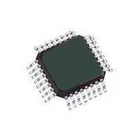
MC68HC908EY16CFA Freescale Semiconductor, MC68HC908EY16CFA Datasheet - Page 120

MC68HC908EY16CFA
Manufacturer Part Number
MC68HC908EY16CFA
Description
IC MCU 16K FLASH 8MHZ SPI 32LQFP
Manufacturer
Freescale Semiconductor
Series
HC08r
Datasheet
1.MC908EY16VFAR2.pdf
(278 pages)
Specifications of MC68HC908EY16CFA
Core Processor
HC08
Core Size
8-Bit
Speed
8MHz
Connectivity
LIN, SCI, SPI
Peripherals
POR, PWM
Number Of I /o
24
Program Memory Size
16KB (16K x 8)
Program Memory Type
FLASH
Ram Size
512 x 8
Voltage - Supply (vcc/vdd)
4.5 V ~ 5.5 V
Data Converters
A/D 8x10b
Oscillator Type
Internal
Operating Temperature
-40°C ~ 85°C
Package / Case
32-LQFP
Processor Series
HC08EY
Core
HC08
Data Bus Width
8 bit
Data Ram Size
512 B
Interface Type
ESCI, SPI
Maximum Clock Frequency
8 MHz
Number Of Programmable I/os
24
Number Of Timers
4
Maximum Operating Temperature
+ 85 C
Mounting Style
SMD/SMT
Development Tools By Supplier
FSICEBASE, M68CBL05CE, ZK-HC08EY-A
Minimum Operating Temperature
- 40 C
On-chip Adc
10 bit, 8 Channel
Lead Free Status / RoHS Status
Contains lead / RoHS non-compliant
Eeprom Size
-
Lead Free Status / Rohs Status
No
Available stocks
Company
Part Number
Manufacturer
Quantity
Price
Company:
Part Number:
MC68HC908EY16CFA
Manufacturer:
FREESCALE
Quantity:
1 831
Company:
Part Number:
MC68HC908EY16CFA
Manufacturer:
QFP
Quantity:
453
Company:
Part Number:
MC68HC908EY16CFA
Manufacturer:
Freescale Semiconductor
Quantity:
10 000
- Current page: 120 of 278
- Download datasheet (2Mb)
Input/Output (I/O) Ports (PORTS)
DDRC[4:0] — Data Direction Register C Bits
Figure 12-9
When bit DDRCx is a 1, reading address $0002 reads the PTCx data latch. When bit DDRCx is a 0,
reading address $0002 reads the voltage level on the pin. The data latch can always be written,
regardless of the state of its data direction bit.
12.5 Port D
Port D is a 2-bit special function port that shares its pins with the timer interface module (TIMA).
12.5.1 Port D Data Register
The port D data register contains a data latch for each of the two port D pins.
120
These read/write bits control port C data direction. Reset clears DDRC[4:0] and MCLKEN, configuring
all port C pins as inputs.
1 = Corresponding port C pin configured as output
0 = Corresponding port C pin configured as input
shows the port C I/O logic.
X = don’t care
Hi-Z = high impedance
1. Writing affects data register, but does not affect input.
DDRC
Bit
Avoid glitches on port C pins by writing to the port C data register before
changing data direction register C bits from 0 to 1.
0
1
0
1
READ DDRC ($0006)
WRITE DDRC ($0006)
WRITE PTC ($0002)
READ PTC ($0002)
PTC
Bit
X
X
2
2
MC68HC908EY16 • MC68HC908EY8 Data Sheet, Rev. 10
Input, Hi-Z
Input, Hi-Z
I/O Pin
Output
Output
Mode
Table 12-3. Port C Pin Functions
RESET
Figure 12-9. Port C I/O Circuit
Accesses to DDRC
Table 12-3
NOTE
Read/Write
DDRCx
DDRC[4:0]
DDRC[4:0]
PTCx
DDRC[7]
DDRC[7]
summarizes the operation of the port C pins.
PTC[4:0]
Read
Pin
Pin
0
Accesses to PTC
PTC[4:0]
PTC[4:0]
Freescale Semiconductor
Write
PTC2
—
PTCx
(1)
Related parts for MC68HC908EY16CFA
Image
Part Number
Description
Manufacturer
Datasheet
Request
R
Part Number:
Description:
Manufacturer:
Freescale Semiconductor, Inc
Datasheet:
Part Number:
Description:
Manufacturer:
Freescale Semiconductor, Inc
Datasheet:
Part Number:
Description:
Manufacturer:
Freescale Semiconductor, Inc
Datasheet:
Part Number:
Description:
Manufacturer:
Freescale Semiconductor, Inc
Datasheet:
Part Number:
Description:
Manufacturer:
Freescale Semiconductor, Inc
Datasheet:
Part Number:
Description:
Manufacturer:
Freescale Semiconductor, Inc
Datasheet:
Part Number:
Description:
Manufacturer:
Freescale Semiconductor, Inc
Datasheet:
Part Number:
Description:
Manufacturer:
Freescale Semiconductor, Inc
Datasheet:
Part Number:
Description:
Manufacturer:
Freescale Semiconductor, Inc
Datasheet:
Part Number:
Description:
Manufacturer:
Freescale Semiconductor, Inc
Datasheet:
Part Number:
Description:
Manufacturer:
Freescale Semiconductor, Inc
Datasheet:
Part Number:
Description:
Manufacturer:
Freescale Semiconductor, Inc
Datasheet:
Part Number:
Description:
Manufacturer:
Freescale Semiconductor, Inc
Datasheet:
Part Number:
Description:
Manufacturer:
Freescale Semiconductor, Inc
Datasheet:
Part Number:
Description:
Manufacturer:
Freescale Semiconductor, Inc
Datasheet:


