MC68HC908EY16CFA Freescale Semiconductor, MC68HC908EY16CFA Datasheet - Page 38
MC68HC908EY16CFA
Manufacturer Part Number
MC68HC908EY16CFA
Description
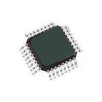
IC MCU 16K FLASH 8MHZ SPI 32LQFP
Manufacturer
Freescale Semiconductor
Series
HC08r
Datasheet
1.MC908EY16VFAR2.pdf
(278 pages)
Specifications of MC68HC908EY16CFA
Core Processor
HC08
Core Size
8-Bit
Speed
8MHz
Connectivity
LIN, SCI, SPI
Peripherals
POR, PWM
Number Of I /o
24
Program Memory Size
16KB (16K x 8)
Program Memory Type
FLASH
Ram Size
512 x 8
Voltage - Supply (vcc/vdd)
4.5 V ~ 5.5 V
Data Converters
A/D 8x10b
Oscillator Type
Internal
Operating Temperature
-40°C ~ 85°C
Package / Case
32-LQFP
Processor Series
HC08EY
Core
HC08
Data Bus Width
8 bit
Data Ram Size
512 B
Interface Type
ESCI, SPI
Maximum Clock Frequency
8 MHz
Number Of Programmable I/os
24
Number Of Timers
4
Maximum Operating Temperature
+ 85 C
Mounting Style
SMD/SMT
Development Tools By Supplier
FSICEBASE, M68CBL05CE, ZK-HC08EY-A
Minimum Operating Temperature
- 40 C
On-chip Adc
10 bit, 8 Channel
Lead Free Status / RoHS Status
Contains lead / RoHS non-compliant
Eeprom Size
-
Lead Free Status / Rohs Status
No
Available stocks
Company
Part Number
Manufacturer
Quantity
Price
Company:

Part Number:
MC68HC908EY16CFA
Manufacturer:
FREESCALE
Quantity:
1 831
Company:
Part Number:
MC68HC908EY16CFA
Manufacturer:
QFP
Quantity:
453
Company:
Part Number:
MC68HC908EY16CFA
Manufacturer:
Freescale Semiconductor
Quantity:
10 000


Memory
2.6.3 FLASH Mass Erase Operation
Use this step-by-step procedure to erase entire FLASH memory to read as logic 1:
38
10. After time, t
1. When in monitor mode, with security sequence failed (see
1. Set both the ERASE bit and the MASS bit in the FLASH control register.
2. Read the FLASH block protect register.
3. Write any data to any FLASH address
4. Wait for a time, t
5. Set the HVEN bit.
6. Wait for a time, t
7. Clear the ERASE and MASS bits.
8. Wait for a time, t
9. Clear the HVEN bit.
stead of any FLASH address.
Mass erase is disabled whenever any block is protected (FLBPR does not
equal $FF).
Programming and erasing of FLASH locations cannot be performed by
code being executed from the FLASH memory. While these operations
must be performed in the order as shown, but other unrelated operations
may occur between the steps.
RCV
(typical 1 µs), the memory can be accessed in read mode again.
NVS
MErase
NVHL
(minimum 10 µs).
MC68HC908EY16 • MC68HC908EY8 Data Sheet, Rev. 10
(minimum 100 µs).
(minimum 4 ms).
(1)
within the FLASH memory address range.
NOTE
NOTE
19.3.2
Security), write to the FLASH block protect register in-
Freescale Semiconductor
Related parts for MC68HC908EY16CFA
Image
Part Number
Description
Manufacturer
Datasheet
Request
R

Part Number:
Description:
Manufacturer:
Freescale Semiconductor, Inc
Datasheet:
Part Number:
Description:
Manufacturer:
Freescale Semiconductor, Inc
Datasheet:
Part Number:
Description:
Manufacturer:
Freescale Semiconductor, Inc
Datasheet:
Part Number:
Description:
Manufacturer:
Freescale Semiconductor, Inc
Datasheet:
Part Number:
Description:
Manufacturer:
Freescale Semiconductor, Inc
Datasheet:
Part Number:
Description:
Manufacturer:
Freescale Semiconductor, Inc
Datasheet:
Part Number:
Description:
Manufacturer:
Freescale Semiconductor, Inc
Datasheet:
Part Number:
Description:
Manufacturer:
Freescale Semiconductor, Inc
Datasheet:
Part Number:
Description:
Manufacturer:
Freescale Semiconductor, Inc
Datasheet:
Part Number:
Description:
Manufacturer:
Freescale Semiconductor, Inc
Datasheet:
Part Number:
Description:
Manufacturer:
Freescale Semiconductor, Inc
Datasheet:
Part Number:
Description:
Manufacturer:
Freescale Semiconductor, Inc
Datasheet:
Part Number:
Description:
Manufacturer:
Freescale Semiconductor, Inc
Datasheet:
Part Number:
Description:
Manufacturer:
Freescale Semiconductor, Inc
Datasheet:
Part Number:
Description:
Manufacturer:
Freescale Semiconductor, Inc
Datasheet: