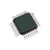
MC68HC908EY16CFA Freescale Semiconductor, MC68HC908EY16CFA Datasheet - Page 37

MC68HC908EY16CFA
Manufacturer Part Number
MC68HC908EY16CFA
Description
IC MCU 16K FLASH 8MHZ SPI 32LQFP
Manufacturer
Freescale Semiconductor
Series
HC08r
Datasheet
1.MC908EY16VFAR2.pdf
(278 pages)
Specifications of MC68HC908EY16CFA
Core Processor
HC08
Core Size
8-Bit
Speed
8MHz
Connectivity
LIN, SCI, SPI
Peripherals
POR, PWM
Number Of I /o
24
Program Memory Size
16KB (16K x 8)
Program Memory Type
FLASH
Ram Size
512 x 8
Voltage - Supply (vcc/vdd)
4.5 V ~ 5.5 V
Data Converters
A/D 8x10b
Oscillator Type
Internal
Operating Temperature
-40°C ~ 85°C
Package / Case
32-LQFP
Processor Series
HC08EY
Core
HC08
Data Bus Width
8 bit
Data Ram Size
512 B
Interface Type
ESCI, SPI
Maximum Clock Frequency
8 MHz
Number Of Programmable I/os
24
Number Of Timers
4
Maximum Operating Temperature
+ 85 C
Mounting Style
SMD/SMT
Development Tools By Supplier
FSICEBASE, M68CBL05CE, ZK-HC08EY-A
Minimum Operating Temperature
- 40 C
On-chip Adc
10 bit, 8 Channel
Lead Free Status / RoHS Status
Contains lead / RoHS non-compliant
Eeprom Size
-
Lead Free Status / Rohs Status
No
Available stocks
Company
Part Number
Manufacturer
Quantity
Price
Company:
Part Number:
MC68HC908EY16CFA
Manufacturer:
FREESCALE
Quantity:
1 831
Company:
Part Number:
MC68HC908EY16CFA
Manufacturer:
QFP
Quantity:
453
Company:
Part Number:
MC68HC908EY16CFA
Manufacturer:
Freescale Semiconductor
Quantity:
10 000
- Current page: 37 of 278
- Download datasheet (2Mb)
2.6.2 FLASH Page Erase Operation
Use this step-by-step procedure to erase a page (64 bytes) of FLASH memory to read as logic 1:
In applications that require more than 1000 program/erase cycles, use the 4 ms page erase specification
to get improved long-term reliability. Any application can use this 4 ms page erase specification. However,
in applications where a FLASH location will be erased and reprogrammed less than 1000 times, and
speed is important, use the 1 ms page erase specification to get a shorter cycle time.
Freescale Semiconductor
10. After time, t
1. Set the ERASE bit and clear the MASS bit in the FLASH control register.
2. Read the FLASH block protect register.
3. Write any data to any FLASH location within the address range of the block to be erased.
4. Wait for a time, t
5. Set the HVEN bit.
6. Wait for a time, t
7. Clear the ERASE bit.
8. Wait for a time, t
9. Clear the HVEN bit.
While these operations must be performed in the order shown, other
unrelated operations may occur between the steps.
Due to the security feature (see
of the FLASH (0xFFDC–0xFFFF), which contains the security bytes,
cannot be erased by Page Erase Operation. It can only be erased with the
Mass Erase Operation.
RCV
(typical 1 µs), the memory can be accessed in read mode again.
NVS
Erase
NVH
(minimum 10 µs).
(minimum 5 µs).
MC68HC908EY16 • MC68HC908EY8 Data Sheet, Rev. 10
(minimum 1 ms or 4 ms).
19.3 Monitor Module
NOTE
NOTE
(MON)) the last page
FLASH Memory (FLASH)
37
Related parts for MC68HC908EY16CFA
Image
Part Number
Description
Manufacturer
Datasheet
Request
R
Part Number:
Description:
Manufacturer:
Freescale Semiconductor, Inc
Datasheet:
Part Number:
Description:
Manufacturer:
Freescale Semiconductor, Inc
Datasheet:
Part Number:
Description:
Manufacturer:
Freescale Semiconductor, Inc
Datasheet:
Part Number:
Description:
Manufacturer:
Freescale Semiconductor, Inc
Datasheet:
Part Number:
Description:
Manufacturer:
Freescale Semiconductor, Inc
Datasheet:
Part Number:
Description:
Manufacturer:
Freescale Semiconductor, Inc
Datasheet:
Part Number:
Description:
Manufacturer:
Freescale Semiconductor, Inc
Datasheet:
Part Number:
Description:
Manufacturer:
Freescale Semiconductor, Inc
Datasheet:
Part Number:
Description:
Manufacturer:
Freescale Semiconductor, Inc
Datasheet:
Part Number:
Description:
Manufacturer:
Freescale Semiconductor, Inc
Datasheet:
Part Number:
Description:
Manufacturer:
Freescale Semiconductor, Inc
Datasheet:
Part Number:
Description:
Manufacturer:
Freescale Semiconductor, Inc
Datasheet:
Part Number:
Description:
Manufacturer:
Freescale Semiconductor, Inc
Datasheet:
Part Number:
Description:
Manufacturer:
Freescale Semiconductor, Inc
Datasheet:
Part Number:
Description:
Manufacturer:
Freescale Semiconductor, Inc
Datasheet:


