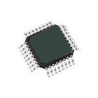
MC68HC908EY16CFA Freescale Semiconductor, MC68HC908EY16CFA Datasheet - Page 25

MC68HC908EY16CFA
Manufacturer Part Number
MC68HC908EY16CFA
Description
IC MCU 16K FLASH 8MHZ SPI 32LQFP
Manufacturer
Freescale Semiconductor
Series
HC08r
Datasheet
1.MC908EY16VFAR2.pdf
(278 pages)
Specifications of MC68HC908EY16CFA
Core Processor
HC08
Core Size
8-Bit
Speed
8MHz
Connectivity
LIN, SCI, SPI
Peripherals
POR, PWM
Number Of I /o
24
Program Memory Size
16KB (16K x 8)
Program Memory Type
FLASH
Ram Size
512 x 8
Voltage - Supply (vcc/vdd)
4.5 V ~ 5.5 V
Data Converters
A/D 8x10b
Oscillator Type
Internal
Operating Temperature
-40°C ~ 85°C
Package / Case
32-LQFP
Processor Series
HC08EY
Core
HC08
Data Bus Width
8 bit
Data Ram Size
512 B
Interface Type
ESCI, SPI
Maximum Clock Frequency
8 MHz
Number Of Programmable I/os
24
Number Of Timers
4
Maximum Operating Temperature
+ 85 C
Mounting Style
SMD/SMT
Development Tools By Supplier
FSICEBASE, M68CBL05CE, ZK-HC08EY-A
Minimum Operating Temperature
- 40 C
On-chip Adc
10 bit, 8 Channel
Lead Free Status / RoHS Status
Contains lead / RoHS non-compliant
Eeprom Size
-
Lead Free Status / Rohs Status
No
Available stocks
Company
Part Number
Manufacturer
Quantity
Price
Company:
Part Number:
MC68HC908EY16CFA
Manufacturer:
FREESCALE
Quantity:
1 831
Company:
Part Number:
MC68HC908EY16CFA
Manufacturer:
QFP
Quantity:
453
Company:
Part Number:
MC68HC908EY16CFA
Manufacturer:
Freescale Semiconductor
Quantity:
10 000
- Current page: 25 of 278
- Download datasheet (2Mb)
Chapter 2
Memory
2.1 Introduction
The M68HC08 central processor unit (CPU08) can address 64 Kbytes of memory space. The memory
map, shown in
2.2 Unimplemented Memory Locations
Accessing an unimplemented location can cause an illegal address reset. In the memory map
(Figure
2.3 Reserved Memory Locations
Accessing a reserved location can have unpredictable effects on microcontroller unit (MCU) operation. In
the
reserved or with the letter R.
2.4 Input/Output (I/O) Section
Most of the control, status, and data registers are in the zero page area of $0000–$003F. Additional I/O
registers have these addresses:
Data registers are shown in
Freescale Semiconductor
•
•
•
•
•
•
•
•
•
•
•
•
•
•
•
Figure 2-1
16 Kbytes of FLASH memory, 15, 872 bytes of user space
512 bytes of random-access memory (RAM)
36 bytes of user-defined vectors
310 bytes of monitor routines in read-only memory (ROM)
1024 bytes of integrated FLASH burn-in routines in ROM
$FE00; SIM break status register, SBSR
$FE01; SIM reset status register, SRSR
$FE03; SIM break flag control register, SBFCR
$FE08; FLASH control register, FLCR
$FE09; break address register high, BRKH
$FE0A; break address register low, BRKL
$FE0B; break status and control register, BRKSCR
$FE0C; LVI status register, LVISR
$FF7E; FLASH block protect register, FLBPR
$FF80; ICG trim value (optional), ICGT
2-1) and in register figures in this document, unimplemented locations are shaded.
and in register figures in this document, reserved locations are marked with the word
Figure
2-1, includes:
MC68HC908EY16 • MC68HC908EY8 Data Sheet, Rev. 10
Figure
2-2. and
Table 2-1
is a list of vector locations.
25
Related parts for MC68HC908EY16CFA
Image
Part Number
Description
Manufacturer
Datasheet
Request
R
Part Number:
Description:
Manufacturer:
Freescale Semiconductor, Inc
Datasheet:
Part Number:
Description:
Manufacturer:
Freescale Semiconductor, Inc
Datasheet:
Part Number:
Description:
Manufacturer:
Freescale Semiconductor, Inc
Datasheet:
Part Number:
Description:
Manufacturer:
Freescale Semiconductor, Inc
Datasheet:
Part Number:
Description:
Manufacturer:
Freescale Semiconductor, Inc
Datasheet:
Part Number:
Description:
Manufacturer:
Freescale Semiconductor, Inc
Datasheet:
Part Number:
Description:
Manufacturer:
Freescale Semiconductor, Inc
Datasheet:
Part Number:
Description:
Manufacturer:
Freescale Semiconductor, Inc
Datasheet:
Part Number:
Description:
Manufacturer:
Freescale Semiconductor, Inc
Datasheet:
Part Number:
Description:
Manufacturer:
Freescale Semiconductor, Inc
Datasheet:
Part Number:
Description:
Manufacturer:
Freescale Semiconductor, Inc
Datasheet:
Part Number:
Description:
Manufacturer:
Freescale Semiconductor, Inc
Datasheet:
Part Number:
Description:
Manufacturer:
Freescale Semiconductor, Inc
Datasheet:
Part Number:
Description:
Manufacturer:
Freescale Semiconductor, Inc
Datasheet:
Part Number:
Description:
Manufacturer:
Freescale Semiconductor, Inc
Datasheet:


