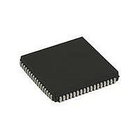
ST16C554DIJ68-F Exar Corporation, ST16C554DIJ68-F Datasheet - Page 10

ST16C554DIJ68-F
Manufacturer Part Number
ST16C554DIJ68-F
Description
IC UART FIFO 16B QUAD 68PLCC
Manufacturer
Exar Corporation
Type
Quad UART with 16-byte FIFOsr
Datasheet
1.ST16C554DCJ68-F.pdf
(39 pages)
Specifications of ST16C554DIJ68-F
Number Of Channels
4, QUART
Package / Case
68-LCC (J-Lead)
Features
*
Fifo's
16 Byte
Protocol
RS232
Voltage - Supply
2.97 V ~ 5.5 V
With Auto Flow Control
Yes
With False Start Bit Detection
Yes
With Modem Control
Yes
With Cmos
Yes
Mounting Type
Surface Mount
Data Rate
1.5 Mbps
Supply Voltage (max)
5.5 V
Supply Voltage (min)
2.97 V
Supply Current
6 mA
Maximum Operating Temperature
+ 85 C
Minimum Operating Temperature
- 40 C
Mounting Style
SMD/SMT
Operating Supply Voltage
3.3 V, 5 V
No. Of Channels
4
Supply Voltage Range
2.97V To 5.5V
Operating Temperature Range
-40°C To +85°C
Digital Ic Case Style
PLCC
No. Of Pins
68
Filter Terminals
SMD
Rohs Compliant
Yes
Lead Free Status / RoHS Status
Lead free / RoHS Compliant
Lead Free Status / RoHS Status
Lead free / RoHS Compliant, Lead free / RoHS Compliant
Other names
1016-1267-5
Available stocks
Company
Part Number
Manufacturer
Quantity
Price
Company:
Part Number:
ST16C554DIJ68-F
Manufacturer:
Exar Corporation
Quantity:
135
Company:
Part Number:
ST16C554DIJ68-F
Manufacturer:
Exar Corporation
Quantity:
10 000
ST16C554/554D
2.97V TO 5.5V QUAD UART WITH 16-BYTE FIFO
loading or unloading the FIFO in a block sequence determined by the programmed trigger level. The following
table show their behavior. Also see
The 554 includes an on-chip oscillator (XTAL1 and XTAL2) to produce a clock for both UART sections in the
device. The CPU data bus does not require this clock for bus operation. The crystal oscillator provides a
system clock to the Baud Rate Generators (BRG) section found in each of the UART. XTAL1 is the input to the
oscillator or external clock buffer input with XTAL2 pin being the output. For programming details, see
“Section 2.8, Programmable Baud Rate Generator” on page 10.
The on-chip oscillator is designed to use an industry standard microprocessor crystal (parallel resonant,
fundamental frequency with 10-22 pF capacitance load, ESR of 20-120 ohms and 100ppm frequency
tolerance) connected externally between the XTAL1 and XTAL2 pins. Typical oscillator connections are shown
in
generator for standard or custom rates. For further reading on oscillator circuit please see application note
DAN108 on EXAR’s web site.
Each UART has its own Baud Rate Generator (BRG) for the transmitter and receiver. The BRG further divides
this clock by a programmable divisor between 1 and (2
data rate. The sampling rate clock is used by the transmitter for data bit shifting and receiver for data sampling.
The BRG divisor is unknown (DLL = 0xXX and DLM = 0xXX) and should be initialized after power up.
Programming the Baud Rate Generator Registers DLL and DLM provides the capability for selecting the
operating data rate.
clock.
F
2.7
2.8
IGURE
Figure
RXRDY#
TXRDY#
P
INS
4. T
Crystal Oscillator or External Clock Input
Programmable Baud Rate Generator
4. Alternatively, an external clock can be connected to the XTAL1 pin to clock the internal baud rate
T
YPICAL
ABLE
LOW = 1 byte
HIGH = no data
LOW = THR empty
HIGH = byte in THR
(FIFO D
5: TXRDY#
FCR
C
Table 6
RYSTAL
BIT
ISABLED
-0=0
C
shows the standard data rates available with a 14.7456MHz crystal or external
AND
ONNECTIONS
)
RXRDY# O
LOW = at least 1 byte in FIFO
HIGH = FIFO empty
LOW = FIFO empty
HIGH = at least 1 byte in FIFO
Figure 17
(DMA M
22-47pF
XTAL1
FCR B
C1
UTPUTS IN
through 22.
ODE
R=300K to 400K
IT
-3 = 0
D
14.7456
ISABLED
MHz
10
16
FIFO
- 1) to obtain a 16X sampling rate clock of the serial
FCR B
)
22-47pF
XTAL2
C2
AND
IT
HIGH to LOW transition when FIFO reaches the
trigger level, or timeout occurs
LOW to HIGH transition when FIFO empties
LOW = FIFO has at least 1 empty location
HIGH = FIFO is full
-0=1 (FIFO E
DMA M
ODE FOR
(DMA M
NABLED
FCR B
C
ODE
)
HANNELS
IT
-3 = 1
E
NABLED
A-D
)
REV. 4.0.1


