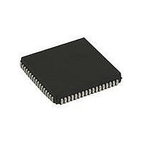
ST16C554DIJ68-F Exar Corporation, ST16C554DIJ68-F Datasheet - Page 3

ST16C554DIJ68-F
Manufacturer Part Number
ST16C554DIJ68-F
Description
IC UART FIFO 16B QUAD 68PLCC
Manufacturer
Exar Corporation
Type
Quad UART with 16-byte FIFOsr
Datasheet
1.ST16C554DCJ68-F.pdf
(39 pages)
Specifications of ST16C554DIJ68-F
Number Of Channels
4, QUART
Package / Case
68-LCC (J-Lead)
Features
*
Fifo's
16 Byte
Protocol
RS232
Voltage - Supply
2.97 V ~ 5.5 V
With Auto Flow Control
Yes
With False Start Bit Detection
Yes
With Modem Control
Yes
With Cmos
Yes
Mounting Type
Surface Mount
Data Rate
1.5 Mbps
Supply Voltage (max)
5.5 V
Supply Voltage (min)
2.97 V
Supply Current
6 mA
Maximum Operating Temperature
+ 85 C
Minimum Operating Temperature
- 40 C
Mounting Style
SMD/SMT
Operating Supply Voltage
3.3 V, 5 V
No. Of Channels
4
Supply Voltage Range
2.97V To 5.5V
Operating Temperature Range
-40°C To +85°C
Digital Ic Case Style
PLCC
No. Of Pins
68
Filter Terminals
SMD
Rohs Compliant
Yes
Lead Free Status / RoHS Status
Lead free / RoHS Compliant
Lead Free Status / RoHS Status
Lead free / RoHS Compliant, Lead free / RoHS Compliant
Other names
1016-1267-5
Available stocks
Company
Part Number
Manufacturer
Quantity
Price
Company:
Part Number:
ST16C554DIJ68-F
Manufacturer:
Exar Corporation
Quantity:
135
Company:
Part Number:
ST16C554DIJ68-F
Manufacturer:
Exar Corporation
Quantity:
10 000
Pin Description
REV. 4.0.1
PIN DESCRIPTIONS
DATA BUS INTERFACE
(R/W#)
(VCC)
(VCC)
CSA#
(CS#)
CSB#
CSC#
CSD#
N
IOW#
IOR#
(A3)
(A4)
A2
A1
A0
D7
D6
D5
D4
D3
D2
D1
D0
AME
64-LQFP
P
22
23
24
60
59
58
57
56
55
54
53
40
11
38
42
IN
9
7
#
68-PLCC
P
32
33
34
68
67
66
52
18
16
20
50
54
IN
5
4
3
2
1
#
T
I/O
YPE
I
I
I
I
I
I
I
Address data lines [2:0]. These 3 address lines select one of the internal regis-
ters in UART channel A-D during a data bus transaction.
Data bus lines [7:0] (bidirectional).
When 16/68# pin is HIGH, the Intel bus interface is selected and this input
becomes read strobe (active low). The falling edge instigates an internal read
cycle and retrieves the data byte from an internal register pointed by the address
lines [A2:A0], puts the data byte on the data bus to allow the host processor to
read it on the rising edge.
When 16/68# pin is LOW, the Motorola bus interface is selected and this input is
not used and should be connected to VCC.
When 16/68# pin is HIGH, it selects Intel bus interface and this input becomes
write strobe (active low). The falling edge instigates the internal write cycle and
the rising edge transfers the data byte on the data bus to an internal register
pointed by the address lines.
When 16/68# pin is LOW, the Motorola bus interface is selected and this input
becomes read (HIGH) and write (LOW) signal.
When 16/68# pin is HIGH, this input is chip select A (active low) to enable chan-
nel A in the device.
When 16/68# pin is LOW, this input becomes the chip select (active low) for the
Motorola bus interface.
When 16/68# pin is HIGH, this input is chip select B (active low) to enable chan-
nel B in the device.
When 16/68# pin is LOW, this input becomes address line A3 which is used for
channel selection in the Motorola bus interface.
When 16/68# pin is HIGH, this input is chip select C (active low) to enable chan-
nel C in the device.
When 16/68# pin is LOW, this input becomes address line A4 which is used for
channel selection in the Motorola bus interface.
When 16/68# pin is HIGH, this input is chip select D (active low) to enable chan-
nel D in the device.
When 16/68# pin is LOW, this input is not used and should be connected VCC.
3
2.97V TO 5.5V QUAD UART WITH 16-BYTE FIFO
D
ESCRIPTION
ST16C554/554D


