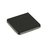
ST16C554DIJ68-F Exar Corporation, ST16C554DIJ68-F Datasheet - Page 19

ST16C554DIJ68-F
Manufacturer Part Number
ST16C554DIJ68-F
Description
IC UART FIFO 16B QUAD 68PLCC
Manufacturer
Exar Corporation
Type
Quad UART with 16-byte FIFOsr
Datasheet
1.ST16C554DCJ68-F.pdf
(39 pages)
Specifications of ST16C554DIJ68-F
Number Of Channels
4, QUART
Package / Case
68-LCC (J-Lead)
Features
*
Fifo's
16 Byte
Protocol
RS232
Voltage - Supply
2.97 V ~ 5.5 V
With Auto Flow Control
Yes
With False Start Bit Detection
Yes
With Modem Control
Yes
With Cmos
Yes
Mounting Type
Surface Mount
Data Rate
1.5 Mbps
Supply Voltage (max)
5.5 V
Supply Voltage (min)
2.97 V
Supply Current
6 mA
Maximum Operating Temperature
+ 85 C
Minimum Operating Temperature
- 40 C
Mounting Style
SMD/SMT
Operating Supply Voltage
3.3 V, 5 V
No. Of Channels
4
Supply Voltage Range
2.97V To 5.5V
Operating Temperature Range
-40°C To +85°C
Digital Ic Case Style
PLCC
No. Of Pins
68
Filter Terminals
SMD
Rohs Compliant
Yes
Lead Free Status / RoHS Status
Lead free / RoHS Compliant
Lead Free Status / RoHS Status
Lead free / RoHS Compliant, Lead free / RoHS Compliant
Other names
1016-1267-5
Available stocks
Company
Part Number
Manufacturer
Quantity
Price
Company:
Part Number:
ST16C554DIJ68-F
Manufacturer:
Exar Corporation
Quantity:
135
Company:
Part Number:
ST16C554DIJ68-F
Manufacturer:
Exar Corporation
Quantity:
10 000
REV. 4.0.1
This register is used to enable the FIFOs, clear the FIFOs, set the receive FIFO trigger levels, and select the
DMA mode. The DMA, and FIFO modes are defined as follows:
FCR[0]: TX and RX FIFO Enable
•
•
FCR[1]: RX FIFO Reset
This bit is only active when FCR bit-0 is a ‘1’.
•
•
FCR[2]: TX FIFO Reset
This bit is only active when FCR bit-0 is a ‘1’.
•
•
FCR[3]: DMA Mode Select
Controls the behavior of the TXRDY# and RXRDY# pins. See DMA operation section for details.
•
•
FCR[5:4]: Reserved (Default 0)
FCR[7:6]: Receive FIFO Trigger Select
(logic 0 = default, RX trigger level =1)
These 2 bits are used to set the trigger level for the receive FIFO. The UART will issue a receive interrupt when
the number of the characters in the FIFO crosses the trigger level.
4.5
Logic 0 = Disable the transmit and receive FIFO (default).
Logic 1 = Enable the transmit and receive FIFOs. This bit must be set to logic 1 when other FCR bits are
written or they will not be programmed.
Logic 0 = No receive FIFO reset (default).
Logic 1 = Reset the receive FIFO pointers and FIFO level counter logic (the receive shift register is not
cleared or altered). This bit will return to a logic 0 after resetting the FIFO.
Logic 0 = No transmit FIFO reset (default).
Logic 1 = Reset the transmit FIFO pointers and FIFO level counter logic (the transmit shift register is not
cleared or altered). This bit will return to a logic 0 after resetting the FIFO.
Logic 0 = Normal Operation (default).
Logic 1 = DMA Mode.
FIFO Control Register (FCR) - Write-Only
T
ABLE
FCR B
0
0
1
1
10: R
IT
-7
ECEIVE
FCR B
FIFO T
0
1
0
1
IT
-6
19
RIGGER
2.97V TO 5.5V QUAD UART WITH 16-BYTE FIFO
R
ECEIVE
L
EVEL
T
Table 10
RIGGER
14
1
4
8
S
ELECTION
L
EVEL
shows the complete selections.
ST16C554/554D


