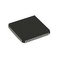
ST16C554DIJ68-F Exar Corporation, ST16C554DIJ68-F Datasheet - Page 21

ST16C554DIJ68-F
Manufacturer Part Number
ST16C554DIJ68-F
Description
IC UART FIFO 16B QUAD 68PLCC
Manufacturer
Exar Corporation
Type
Quad UART with 16-byte FIFOsr
Datasheet
1.ST16C554DCJ68-F.pdf
(39 pages)
Specifications of ST16C554DIJ68-F
Number Of Channels
4, QUART
Package / Case
68-LCC (J-Lead)
Features
*
Fifo's
16 Byte
Protocol
RS232
Voltage - Supply
2.97 V ~ 5.5 V
With Auto Flow Control
Yes
With False Start Bit Detection
Yes
With Modem Control
Yes
With Cmos
Yes
Mounting Type
Surface Mount
Data Rate
1.5 Mbps
Supply Voltage (max)
5.5 V
Supply Voltage (min)
2.97 V
Supply Current
6 mA
Maximum Operating Temperature
+ 85 C
Minimum Operating Temperature
- 40 C
Mounting Style
SMD/SMT
Operating Supply Voltage
3.3 V, 5 V
No. Of Channels
4
Supply Voltage Range
2.97V To 5.5V
Operating Temperature Range
-40°C To +85°C
Digital Ic Case Style
PLCC
No. Of Pins
68
Filter Terminals
SMD
Rohs Compliant
Yes
Lead Free Status / RoHS Status
Lead free / RoHS Compliant
Lead Free Status / RoHS Status
Lead free / RoHS Compliant, Lead free / RoHS Compliant
Other names
1016-1267-5
Available stocks
Company
Part Number
Manufacturer
Quantity
Price
Company:
Part Number:
ST16C554DIJ68-F
Manufacturer:
Exar Corporation
Quantity:
135
Company:
Part Number:
ST16C554DIJ68-F
Manufacturer:
Exar Corporation
Quantity:
10 000
REV. 4.0.1
LCR[5]: TX and RX Parity Select
If the parity bit is enabled, LCR BIT-5 selects the forced parity format.
•
•
•
LCR[6]: Transmit Break Enable
When enabled, the Break control bit causes a break condition to be transmitted (the TX output is forced to a
“space’, logic 0, state). This condition remains, until disabled by setting LCR bit-6 to a logic 0.
•
•
LCR[7]: Baud Rate Divisors Enable
Baud rate generator divisor (DLL/DLM) enable.
•
•
The MCR register is used for controlling the serial/modem interface signals or general purpose inputs/outputs.
MCR[0]: DTR# Output
The DTR# pin is a modem control output. If the modem interface is not used, this output may be used as a
general purpose output.
•
•
MCR[1]: RTS# Output
The RTS# pin is a modem control output. If the modem interface is not used, this output may be used as a
general purpose output.
•
•
MCR[2]: Reserved
OP1# is not available as an output pin on the 554. But it is available for use during Internal Loopback Mode. In
the Loopback Mode, this bit is used to write the state of the modem RI# interface signal.
4.7
LCR BIT-5 = logic 0, parity is not forced (default).
LCR BIT-5 = logic 1 and LCR BIT-4 = logic 0, parity bit is forced to HIGH for the transmit and receive data.
LCR BIT-5 = logic 1 and LCR BIT-4 = logic 1, parity bit is forced to LOW for the transmit and receive data.
Logic 0 = No TX break condition. (default)
Logic 1 = Forces the transmitter output (TX) to a “space”, logic 0, for alerting the remote receiver of a line
break condition.
Logic 0 = Data registers are selected (default).
Logic 1 = Divisor latch registers are selected.
Logic 0 = Force DTR# output HIGH (default).
Logic 1 = Force DTR# output LOW.
Logic 0 = Force RTS# output HIGH (default).
Logic 1 = Force RTS# output LOW.
Modem Control Register (MCR) or General Purpose Outputs Control - Read/Write
LCR B
X
0
0
1
1
IT
-5 LCR B
X
0
1
0
1
T
ABLE
IT
-4 LCR B
11: P
0
1
1
1
1
ARITY SELECTION
IT
21
-3
2.97V TO 5.5V QUAD UART WITH 16-BYTE FIFO
Forced parity to space, LOW
Force parity to mark, HIGH
P
ARITY SELECTION
Even parity
Odd parity
No parity
ST16C554/554D


