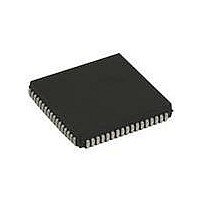
ST16C554DIJ68-F Exar Corporation, ST16C554DIJ68-F Datasheet - Page 22

ST16C554DIJ68-F
Manufacturer Part Number
ST16C554DIJ68-F
Description
IC UART FIFO 16B QUAD 68PLCC
Manufacturer
Exar Corporation
Type
Quad UART with 16-byte FIFOsr
Datasheet
1.ST16C554DCJ68-F.pdf
(39 pages)
Specifications of ST16C554DIJ68-F
Number Of Channels
4, QUART
Package / Case
68-LCC (J-Lead)
Features
*
Fifo's
16 Byte
Protocol
RS232
Voltage - Supply
2.97 V ~ 5.5 V
With Auto Flow Control
Yes
With False Start Bit Detection
Yes
With Modem Control
Yes
With Cmos
Yes
Mounting Type
Surface Mount
Data Rate
1.5 Mbps
Supply Voltage (max)
5.5 V
Supply Voltage (min)
2.97 V
Supply Current
6 mA
Maximum Operating Temperature
+ 85 C
Minimum Operating Temperature
- 40 C
Mounting Style
SMD/SMT
Operating Supply Voltage
3.3 V, 5 V
No. Of Channels
4
Supply Voltage Range
2.97V To 5.5V
Operating Temperature Range
-40°C To +85°C
Digital Ic Case Style
PLCC
No. Of Pins
68
Filter Terminals
SMD
Rohs Compliant
Yes
Lead Free Status / RoHS Status
Lead free / RoHS Compliant
Lead Free Status / RoHS Status
Lead free / RoHS Compliant, Lead free / RoHS Compliant
Other names
1016-1267-5
Available stocks
Company
Part Number
Manufacturer
Quantity
Price
Company:
Part Number:
ST16C554DIJ68-F
Manufacturer:
Exar Corporation
Quantity:
135
Company:
Part Number:
ST16C554DIJ68-F
Manufacturer:
Exar Corporation
Quantity:
10 000
ST16C554/554D
2.97V TO 5.5V QUAD UART WITH 16-BYTE FIFO
MCR[3]: INT Output Enable
Enable or disable INT outputs to become active or in three-state. This function is associated with the INTSEL
input, see below table for details. This bit is also used to control the OP2# signal during internal loopback
mode. INTSEL pin must be LOW during 68 mode.
•
•
MCR[4]: Internal Loopback Enable
•
•
MCR[7:5]: Reserved (Default 0)
This register is writeable but it is not recommended. The LSR provides the status of data transfers between the
UART and the host. If IER bit-2 is enabled, LSR bit-1 will generate an interrupt immediately and LSR bits 2-4
will generate an interrupt when a character with an error is in the RHR.
LSR[0]: Receive Data Ready Indicator
•
•
LSR[1]: Receiver Overrun Flag
•
•
LSR[2]: Receive Data Parity Error Tag
•
•
LSR[3]: Receive Data Framing Error Tag
•
•
4.8
Logic 0 = INT (A-D) outputs disabled (three state) in the 16 mode (default). During internal loopback mode,
OP2# is HIGH.
Logic 1 = INT (A-D) outputs enabled (active) in the 16 mode. During internal loopback mode, OP2# is LOW.
Logic 0 = Disable loopback mode (default).
Logic 1 = Enable local loopback mode, see loopback section and
Logic 0 = No data in receive holding register or FIFO (default).
Logic 1 = Data has been received and can be read from the receive holding register or RX FIFO.
Logic 0 = No overrun error (default).
Logic 1 = Overrun error. A data overrun error condition occurred in the receive shift register. This happens
when additional data arrives while the FIFO is full. In this case the previous data in the receive shift register
is overwritten. Note that under this condition the data byte in the receive shift register is not transferred into
the FIFO, therefore the data in the FIFO is not corrupted by the error.
Logic 0 = No parity error (default).
Logic 1 = Parity error. The receive character in RHR does not have correct parity information and is suspect.
This error is associated with the character available for reading in RHR.
Logic 0 = No framing error (default).
Logic 1 = Framing error. The receive character did not have a valid stop bit(s). This error is associated with
the character available for reading in RHR.
Line Status Register (LSR) - Read/Write
INTSEL
P
0
0
1
IN
B
MCR
T
IT
X
0
1
ABLE
-3
12: INT O
INT A-D O
22
UTPUT
Three-State
UTPUTS IN
Active
Active
M
ODES
Figure
16 M
ODE
10.
REV. 4.0.1


