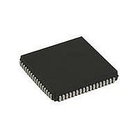
ST16C554DIJ68-F Exar Corporation, ST16C554DIJ68-F Datasheet - Page 9

ST16C554DIJ68-F
Manufacturer Part Number
ST16C554DIJ68-F
Description
IC UART FIFO 16B QUAD 68PLCC
Manufacturer
Exar Corporation
Type
Quad UART with 16-byte FIFOsr
Datasheet
1.ST16C554DCJ68-F.pdf
(39 pages)
Specifications of ST16C554DIJ68-F
Number Of Channels
4, QUART
Package / Case
68-LCC (J-Lead)
Features
*
Fifo's
16 Byte
Protocol
RS232
Voltage - Supply
2.97 V ~ 5.5 V
With Auto Flow Control
Yes
With False Start Bit Detection
Yes
With Modem Control
Yes
With Cmos
Yes
Mounting Type
Surface Mount
Data Rate
1.5 Mbps
Supply Voltage (max)
5.5 V
Supply Voltage (min)
2.97 V
Supply Current
6 mA
Maximum Operating Temperature
+ 85 C
Minimum Operating Temperature
- 40 C
Mounting Style
SMD/SMT
Operating Supply Voltage
3.3 V, 5 V
No. Of Channels
4
Supply Voltage Range
2.97V To 5.5V
Operating Temperature Range
-40°C To +85°C
Digital Ic Case Style
PLCC
No. Of Pins
68
Filter Terminals
SMD
Rohs Compliant
Yes
Lead Free Status / RoHS Status
Lead free / RoHS Compliant
Lead Free Status / RoHS Status
Lead free / RoHS Compliant, Lead free / RoHS Compliant
Other names
1016-1267-5
Available stocks
Company
Part Number
Manufacturer
Quantity
Price
Company:
Part Number:
ST16C554DIJ68-F
Manufacturer:
Exar Corporation
Quantity:
135
Company:
Part Number:
ST16C554DIJ68-F
Manufacturer:
Exar Corporation
Quantity:
10 000
REV. 4.0.1
Each UART channel in the 554 has a set of enhanced registers for controlling, monitoring and data loading and
unloading. The configuration register set is compatible to those already available in the standard single
16C550. These registers function as data holding registers (THR/RHR), interrupt status and control registers
(ISR/IER), a FIFO control register (FCR), receive line status and control registers (LSR/LCR), modem status
and control registers (MSR/MCR), programmable data rate (clock) divisor registers (DLL/DLM), and a user
accessible scratchpad register (SPR). All the register functions are discussed in full detail later in
3.0, UART INTERNAL REGISTERS” on page
The interrupt outputs change according to the operating mode and enhanced features setup.
summarize the operating behavior for the transmitter and receiver. Also see
The device does not support direct memory access. The DMA Mode (a legacy term) in this document does not
mean “direct memory access” but refers to data block transfer operation. The DMA mode affects the state of
the RXRDY# A-D and TXRDY# A-D output pins. The transmit and receive FIFO trigger levels provide
additional flexibility to the user for block mode operation. The LSR bits 5-6 provide an indication when the
transmitter is empty or has an empty location(s) for more data. The user can optionally operate the transmit
and receive FIFO in the DMA mode (FCR bit-3 = 1). When the transmit and receive FIFOs are enabled and the
DMA mode is disabled (FCR bit-3 = 0), the 554 is placed in single-character mode for data transmit or receive
operation. When DMA mode is enabled (FCR bit-3 = 1), the user takes advantage of block mode operation by
2.4
2.5
2.6
INT Pin
INT Pin
Channels A-D Internal Registers
INT Ouputs for Channels A-D
DMA Mode
LOW = a byte in THR
HIGH = THR empty
LOW = no data
HIGH = 1 byte
(FIFO D
(FIFO D
FCR B
FCR B
T
ABLE
T
ABLE
IT
ISABLED
IT
ISABLED
-0 = 0
-0 = 0
3: INT P
4: INT P
)
)
IN
IN
O
LOW = FIFO above trigger level
HIGH = FIFO below trigger level or
FIFO empty
LOW = FIFO below trigger level
HIGH = FIFO above trigger level
PERATION FOR
O
PERATION FOR
(DMA Mode Disabled)
(DMA Mode Disabled)
15.
FCR Bit-3 = 0
FCR Bit-3 = 0
9
T
RANSMITTER FOR
R
2.97V TO 5.5V QUAD UART WITH 16-BYTE FIFO
ECEIVER FOR
FCR B
FCR B
IT
IT
-0 = 1 (FIFO E
-0 = 1 (FIFO E
C
HANNELS
C
HANNELS
LOW = FIFO above trigger level
HIGH = FIFO below trigger level or
FIFO empty
LOW = FIFO below trigger level
HIGH = FIFO above trigger level
Figure 17
NABLED
NABLED
(DMA Mode Enabled)
(DMA Mode Enabled)
A-D
A-D
FCR Bit-3 = 1
FCR Bit-3 = 1
through 22.
)
)
ST16C554/554D
Table 3 and 4
“Section


