1321XDSK-BDM Freescale Semiconductor, 1321XDSK-BDM Datasheet - Page 11
1321XDSK-BDM
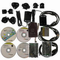
Manufacturer Part Number
1321XDSK-BDM
Description
KIT STARTER DEV 1321X W/USB
Manufacturer
Freescale Semiconductor
Type
Sensor Demor
Specifications of 1321XDSK-BDM
Frequency
2.4GHz
Wireless Frequency
2.4 GHz
Interface Type
SPI
Modulation
DSSS OQPSK
Security
128 bit AES
Operating Voltage
2 VDC to 3.4 VDC
Output Power
2 dBm
Antenna
F-Antenna
Operating Temperature Range
- 40 C to + 85 C
For Use With/related Products
MC1321x
Lead Free Status / RoHS Status
Contains lead / RoHS compliant by exemption


Freescale Semiconductor
Pin #
38
39
40
41
42
43
44
45
46
47
48
49
50
51
52
53
54
55
56
PAO_P
PAO_M
SM
GPIO4
GPIO3
GPIO2
GPIO1
VDD
ATTN
PTD2/TPM1CH2
PTD4/TPM2CH1
PTD5/TPM2CH2
PTD6/TPM2CH3
PTD7/TPM2CH4
PTB0/AD1P0
PTB1/AD1P1
PTB2/AD1P2
PTB3/AD1P3
PTB4/AD1P4
Pin Name
2
1
1
RF Output
RF Output
Input
Digital Input/
Output
Digital
Input/Output
Test Point
Test Point
Power Input
Digital Input
Digital
Input/Output
Digital
Input/Output
Digital
Input/Output
Digital
Input/Output
Digital
Input/Output
Input/Output
Input/Output
Input/Output
Input/Output
Input/Output
Type
Table 2. Pin Function Description (continued)
MC13211/212/213 Technical Data, Rev. 1.8
Modem power amplifier RF
output positive
Modem power amplifier RF
output negative
Test Mode pin
General Purpose
Input/Output 4.
Modem General Purpose
Input/Output 3
MCU Port E Bit 6 / Modem
General Purpose
Input/Output 2
MCU Port E Bit 7 / Modem
General Purpose
Input/Output 1
MCU main power supply
Active Low Attention.
Transitions IC from either
Hibernate or Doze Modes
to Idle.
MCU Port D Bit 2 / TPM1
Channel 2
MCU Port D Bit 4 / TPM2
Channel 1
MCU Port D Bit 5 / TPM2
Channel 2
MCU Port D Bit 6 / TPM2
Channel 3
MCU Port D Bit 7 / TPM2
Channel 4
MCU Port B Bit 0 / ATD
analogChannel 0
MCU Port B Bit 1 / ATD
analog Channel 1
MCU Port B Bit 2 / ATD
analog Channel 2
MCU Port B Bit 3 / ATD
analog Channel 3
MCU Port B Bit 4 / ATD
analog Channel 4
Description
Open drain. Connect to VDDA through a bias
network when used with external balun. Not used
when internal T/R switch is used.
Open drain. Connect to VDDA through a bias
network when used with external balun. Not used
when internal T/R switch is used.
Must be grounded for normal operation
See Footnote 1
See Footnote 1
Internally connected pins. When gpio_alt_en,
Register 9, Bit 7 = 1, GPIO2 functions as a “CRC
Valid” indicator.
Internally connected pins. When gpio_alt_en,
Register 9, Bit 7 = 1, GPIO1 functions as an “Out of
Idle” indicator.
Decouple to ground.
See Footnote 2
Functionality
11
Related parts for 1321XDSK-BDM
Image
Part Number
Description
Manufacturer
Datasheet
Request
R

Part Number:
Description:
KIT STARTER DEVELOPER 1321X
Manufacturer:
Freescale Semiconductor
Datasheet:

Part Number:
Description:
Manufacturer:
Freescale Semiconductor, Inc
Datasheet:
Part Number:
Description:
Manufacturer:
Freescale Semiconductor, Inc
Datasheet:
Part Number:
Description:
Manufacturer:
Freescale Semiconductor, Inc
Datasheet:
Part Number:
Description:
Manufacturer:
Freescale Semiconductor, Inc
Datasheet:
Part Number:
Description:
Manufacturer:
Freescale Semiconductor, Inc
Datasheet:
Part Number:
Description:
Manufacturer:
Freescale Semiconductor, Inc
Datasheet:
Part Number:
Description:
Manufacturer:
Freescale Semiconductor, Inc
Datasheet:
Part Number:
Description:
Manufacturer:
Freescale Semiconductor, Inc
Datasheet:
Part Number:
Description:
Manufacturer:
Freescale Semiconductor, Inc
Datasheet:
Part Number:
Description:
Manufacturer:
Freescale Semiconductor, Inc
Datasheet:
Part Number:
Description:
Manufacturer:
Freescale Semiconductor, Inc
Datasheet:
Part Number:
Description:
Manufacturer:
Freescale Semiconductor, Inc
Datasheet:
Part Number:
Description:
Manufacturer:
Freescale Semiconductor, Inc
Datasheet:
Part Number:
Description:
Manufacturer:
Freescale Semiconductor, Inc
Datasheet: