1321XDSK-BDM Freescale Semiconductor, 1321XDSK-BDM Datasheet - Page 58
1321XDSK-BDM
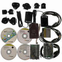
Manufacturer Part Number
1321XDSK-BDM
Description
KIT STARTER DEV 1321X W/USB
Manufacturer
Freescale Semiconductor
Type
Sensor Demor
Specifications of 1321XDSK-BDM
Frequency
2.4GHz
Wireless Frequency
2.4 GHz
Interface Type
SPI
Modulation
DSSS OQPSK
Security
128 bit AES
Operating Voltage
2 VDC to 3.4 VDC
Output Power
2 dBm
Antenna
F-Antenna
Operating Temperature Range
- 40 C to + 85 C
For Use With/related Products
MC1321x
Lead Free Status / RoHS Status
Contains lead / RoHS compliant by exemption


1
2
3
4
5
6
7
6.4
This section describes ac timing characteristics for each peripheral system.
6.4.1
58
ICGOUT period jitter,
Internal oscillator deviation from trimmed frequency
Bus frequency (t
Real-time interrupt internal oscillator period
External reset pulse width
Reset low drive
Active background debug mode latch setup time
Active background debug mode latch hold time
IRQ pulse width
Port rise and fall time (load = 50 pF)
Self-clocked mode frequency is the frequency that the DCO generates when the FLL is open-loop.
Loss of reference frequency is the reference frequency detected internally, which transitions the ICG into self-clocked mode if
it is not in the desired range.
Loss of DCO frequency is the DCO frequency detected internally, which transitions the ICG into FLL bypassed external mode
(if an external reference exists) if it is not in the desired range.
This parameter is characterized before qualification rather than 100% tested.
Proper PC board layout procedures must be followed to achieve specifications.
This specification applies to the period of time required for the FLL to lock after entering FLL engaged internal or external
modes. If a crystal/resonator is being used as the reference, this specification assumes it is already running.
Jitter is the average deviation from the programmed frequency measured over the specified interval at maximum f
Measurements are made with the device powered by filtered supplies and clocked by a stable external clock signal. Noise
injected into the FLL circuitry via V
for a given interval.
Long term jitter (averaged over 2 ms interval)
V
V
Slew rate control disabled
Slew rate control enabled
DD
DD
= 1.8 – 3.6 V, (constant temperature)
= 3.0 V ±10%, –40° C to 85° C
MCU AC Peripheral Characteristics
MCU Control Timing
(V
2
3
cyc
DDA
= 1/f
Characteristic
4, 7
= V
Bus
measured at f
Parameter
1
DDA
)
Table 17. MCU ICG Frequency Specifications (continued)
(min) to V
DDA
4
ICGOUT
MC13211/212/213 Technical Data, Rev. 1.8
and V
DDA
Table 18. MCU Control Timing
SSA
Max
(max), Temperature Range = –40 to 85°C Ambient)
and variation in crystal oscillator frequency increase the C
Symbol
ACC
C
Jitter
t
Symbol
Rise
t
t
t
int
MSSU
t
t
f
extrst
rstdrv
t
MSH
Bus
ILIH
RTI
, t
Fall
Min
—
—
—
f
f
1.5 x t
Self_reset
Self_reset
1.5 x
34 x
Min
700
25
25
dc
—
—
cyc
Typical
± 0.5
±0.5
Typical
—
30
3
Freescale Semiconductor
Max
0.2
±2
±2
1300
Max
20
—
—
—
—
—
Jitter
percentage
ICGOUT
% f
Unit
%
MHz
Unit
ICG
μs
ns
ns
ns
ns
ns
ns
.
Related parts for 1321XDSK-BDM
Image
Part Number
Description
Manufacturer
Datasheet
Request
R

Part Number:
Description:
KIT STARTER DEVELOPER 1321X
Manufacturer:
Freescale Semiconductor
Datasheet:

Part Number:
Description:
Manufacturer:
Freescale Semiconductor, Inc
Datasheet:
Part Number:
Description:
Manufacturer:
Freescale Semiconductor, Inc
Datasheet:
Part Number:
Description:
Manufacturer:
Freescale Semiconductor, Inc
Datasheet:
Part Number:
Description:
Manufacturer:
Freescale Semiconductor, Inc
Datasheet:
Part Number:
Description:
Manufacturer:
Freescale Semiconductor, Inc
Datasheet:
Part Number:
Description:
Manufacturer:
Freescale Semiconductor, Inc
Datasheet:
Part Number:
Description:
Manufacturer:
Freescale Semiconductor, Inc
Datasheet:
Part Number:
Description:
Manufacturer:
Freescale Semiconductor, Inc
Datasheet:
Part Number:
Description:
Manufacturer:
Freescale Semiconductor, Inc
Datasheet:
Part Number:
Description:
Manufacturer:
Freescale Semiconductor, Inc
Datasheet:
Part Number:
Description:
Manufacturer:
Freescale Semiconductor, Inc
Datasheet:
Part Number:
Description:
Manufacturer:
Freescale Semiconductor, Inc
Datasheet:
Part Number:
Description:
Manufacturer:
Freescale Semiconductor, Inc
Datasheet:
Part Number:
Description:
Manufacturer:
Freescale Semiconductor, Inc
Datasheet: