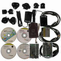
1321XDSK-BDM Freescale Semiconductor, 1321XDSK-BDM Datasheet - Page 23

1321XDSK-BDM
Manufacturer Part Number
1321XDSK-BDM
Description
KIT STARTER DEV 1321X W/USB
Manufacturer
Freescale Semiconductor
Type
Sensor Demor
Specifications of 1321XDSK-BDM
Frequency
2.4GHz
Wireless Frequency
2.4 GHz
Interface Type
SPI
Modulation
DSSS OQPSK
Security
128 bit AES
Operating Voltage
2 VDC to 3.4 VDC
Output Power
2 dBm
Antenna
F-Antenna
Operating Temperature Range
- 40 C to + 85 C
For Use With/related Products
MC1321x
Lead Free Status / RoHS Status
Contains lead / RoHS compliant by exemption
15-8 (xtal_trim[7:0]). The trimming procedure varies the frequency by a few hertz per step, depending on
the type of crystal. The high end of the frequency spectrum is set when xtal_trim[7:0] is set to zero. As
xtal_trim[7:0] is increased, the frequency is decreased. Accuracy of this feature can be observed by
varying xtal_trim[7:0] and using a spectrum analyzer or frequency counter to track the change in
frequency of the crystal signal. The reference oscillator frequency can be measured at the CLKO contact
by programming CLKO_Ctl Register 0A, Bits 2-0, to value 000.
Figure 13
4.8
The MC1321x RF analog interface has been designed to provide maximum flexibility as well as low
external part count and cost. An on-chip transmit/receive (T/R) switch with bias switch (CT_Bias) can be
used for a simple single antenna interface with a balun. Alternately, separate full differential RFIN and
PAO outputs can be utilized for separate RX and TX antennae or external LNA and PA designs.
Figure 14
Freescale Semiconductor
1.
2.
Figure 14A
used. The balun converts the single-ended antenna to differential signals that interface to the
RFIN_x (PAO_x) pins of the radio. The CT_Bias pin provides the proper bias point to the balun
depending on operation, that is, CT_Bias is at VDDA voltage for transmit and is at ground for
receive. The internal T/R switch enables the signal to an onboard LNA for receive and enables the
onboard PAs for transmit.
Figure 14B
greater range. An external antenna switch is used to multiplex the antenna between receive and
transmit. An LNA is in the receive path to add gain for greater receive sensitivity. Two external
baluns are required to convert the single-ended antenna switch signals to the differential signals
Radio Usage
shows typical oscillator frequency decrease versus the value programmed in xtal_trim[7:0].
shows three possible configurations for the transceiver radio RF usage.
shows a single antenna configuration with an external low noise amplifier (LNA) for
shows a single antenna configuration in which the MC1321x internal T/R switch is
Figure 13. Crystal Frequency Variation vs. xtal_trim[7:0]
-200
-300
-400
-500
-600
-700
-800
-900
-100
0
0
MC13211/212/213 Technical Data, Rev. 1.8
50
xtal_trim[7:0] (decimal)
100
150
200
250
300
23


