1321XDSK-BDM Freescale Semiconductor, 1321XDSK-BDM Datasheet - Page 26
1321XDSK-BDM
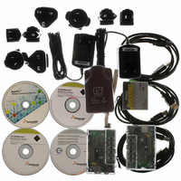
Manufacturer Part Number
1321XDSK-BDM
Description
KIT STARTER DEV 1321X W/USB
Manufacturer
Freescale Semiconductor
Type
Sensor Demor
Specifications of 1321XDSK-BDM
Frequency
2.4GHz
Wireless Frequency
2.4 GHz
Interface Type
SPI
Modulation
DSSS OQPSK
Security
128 bit AES
Operating Voltage
2 VDC to 3.4 VDC
Output Power
2 dBm
Antenna
F-Antenna
Operating Temperature Range
- 40 C to + 85 C
For Use With/related Products
MC1321x
Lead Free Status / RoHS Status
Contains lead / RoHS compliant by exemption


5.2
The MCU has multiple operational modes to facilitate maximum system performance while also providing
low-power modes. In the MC1321x, the MCU can use the following modes:
5.2.1
This is the normal operating mode for the HCS08. This mode is selected when the BKGD/MS pin is high
at the rising edge of reset. In this mode, the CPU executes code from internal memory with execution
beginning at the address fetched from memory at $FFFE:$FFFF after reset.
5.2.2
Wait Mode is entered by executing a WAIT instruction. Upon execution of the WAIT instruction, the CPU
enters a low-power state in which it is not clocked. The I bit in CCR is cleared when the CPU enters the
wait mode, enabling interrupts. When an interrupt request occurs, the CPU exits the wait mode and
resumes processing, beginning with the stacking operations leading to the interrupt service routine.
While the MCU is in Wait Mode, there are some restrictions on which background debug commands can
be used. Only the BACKGROUND command and memory-access-with-status commands are available
when the MCU is in wait mode. The memory-access-with-status commands do not allow memory access,
but they report an error indicating that the MCU is in either stop or wait mode. The BACKGROUND
command can be used to wake the MCU from Wait Mode and enter active background mode.
5.2.3
The Stop2 Mode provides very low standby power consumption and maintains the contents of RAM and
the current state of all of the I/O pins. Stop2 can be entered only if the LVD circuit is not enabled in Stop
Modes (either LVDE or LVDSE not set).
26
•
•
•
•
Run
Wait
Stop2
Stop3
MCU Modes of Operation
Run Mode
Wait Mode
Stop 2
•
•
The MCU can also be programmed for Stop1 mode, but this mode IS
NOT USABLE. The reset to the modem function is controlled by an
MCU GPIO and the GPIO state must be maintained during the MCU
“stop” condition. Stop1 mode does not control I/O states as required
during modem power down condition.
To attain specified Stop2 and Stop3 currents, all unused port signals
must be programmed to a known state (recommended as outputs in the
low state)
MC13211/212/213 Technical Data, Rev. 1.8
NOTE
Freescale Semiconductor
Related parts for 1321XDSK-BDM
Image
Part Number
Description
Manufacturer
Datasheet
Request
R

Part Number:
Description:
KIT STARTER DEVELOPER 1321X
Manufacturer:
Freescale Semiconductor
Datasheet:

Part Number:
Description:
Manufacturer:
Freescale Semiconductor, Inc
Datasheet:
Part Number:
Description:
Manufacturer:
Freescale Semiconductor, Inc
Datasheet:
Part Number:
Description:
Manufacturer:
Freescale Semiconductor, Inc
Datasheet:
Part Number:
Description:
Manufacturer:
Freescale Semiconductor, Inc
Datasheet:
Part Number:
Description:
Manufacturer:
Freescale Semiconductor, Inc
Datasheet:
Part Number:
Description:
Manufacturer:
Freescale Semiconductor, Inc
Datasheet:
Part Number:
Description:
Manufacturer:
Freescale Semiconductor, Inc
Datasheet:
Part Number:
Description:
Manufacturer:
Freescale Semiconductor, Inc
Datasheet:
Part Number:
Description:
Manufacturer:
Freescale Semiconductor, Inc
Datasheet:
Part Number:
Description:
Manufacturer:
Freescale Semiconductor, Inc
Datasheet:
Part Number:
Description:
Manufacturer:
Freescale Semiconductor, Inc
Datasheet:
Part Number:
Description:
Manufacturer:
Freescale Semiconductor, Inc
Datasheet:
Part Number:
Description:
Manufacturer:
Freescale Semiconductor, Inc
Datasheet:
Part Number:
Description:
Manufacturer:
Freescale Semiconductor, Inc
Datasheet: