1321XDSK-BDM Freescale Semiconductor, 1321XDSK-BDM Datasheet - Page 27
1321XDSK-BDM
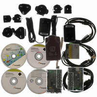
Manufacturer Part Number
1321XDSK-BDM
Description
KIT STARTER DEV 1321X W/USB
Manufacturer
Freescale Semiconductor
Type
Sensor Demor
Specifications of 1321XDSK-BDM
Frequency
2.4GHz
Wireless Frequency
2.4 GHz
Interface Type
SPI
Modulation
DSSS OQPSK
Security
128 bit AES
Operating Voltage
2 VDC to 3.4 VDC
Output Power
2 dBm
Antenna
F-Antenna
Operating Temperature Range
- 40 C to + 85 C
For Use With/related Products
MC1321x
Lead Free Status / RoHS Status
Contains lead / RoHS compliant by exemption


Before entering Stop2 Mode, the user must save the contents of the I/O port registers, as well as any other
memory-mapped registers they want to restore after exit of Stop2, to locations in RAM. Upon exit of
Stop2, these values can be restored by user software before pin latches are opened.
When the MCU is in Stop2 Mode, all internal circuits that are powered from the voltage regulator are
turned off, except for the RAM. The voltage regulator is in a low-power standby state, as is the ATD. Upon
entry into Stop2, the states of the I/O pins are latched. The states are held while in Stop2 Mode and after
exiting Stop2 Mode until a 1 is written to PPDACK in SPMSC2.
Exit from Stop2 is performed by asserting either of the wake-up pins: RESET or IRQ, or by an RTI
interrupt. IRQ is always an active low input when the MCU is in Stop2, regardless of how it was
configured before entering Stop2.
Upon wake-up from Stop2 Mode, the MCU will start up as from a power-on reset (POR) except pin states
remain latched. The CPU will take the reset vector. The system and all peripherals will be in their default
reset states and must be initialized.
After waking up from Stop2, the PPDF bit in SPMSC2 is set. This flag may be used to direct user code to
go to a Stop2 recovery routine. PPDF remains set and the I/O pin states remain latched until a 1 is written
to PPDACK in SPMSC2.
To maintain I/O state for pins that were configured as general-purpose I/O, the user must restore the
contents of the I/O port registers, which have been saved in RAM, to the port registers before writing to
the PPDACK bit. If the port registers are not restored from RAM before writing to PPDACK, then the
register bits will assume their reset states when the I/O pin latches are opened and the I/O pins will switch
to their reset states.
For pins that were configured as peripheral I/O, the user must reconfigure the peripheral module that
interfaces to the pin before writing to the PPDACK bit. If the peripheral module is not enabled before
writing to PPDACK, the pins will be controlled by their associated port control registers when the I/O
latches are opened.
A separate self-clocked source (approximately 1 kHz) for the real-time interrupt allows a walk-up from
Stop2 or Stop3 Modes with no external components. When RTIS2:RTIS1:RTIS0 = 0:0:0, the real-time
interrupt function and this 1-kHz source are disabled. Power consumption is lower when the 1-kHz source
is disabled, but in that case the real-time interrupt cannot wake the MCU from stop.
5.2.4
Stop3
Upon entering the Stop3 Mode, all of the clocks in the MCU, including the oscillator itself, are halted. The
ICG is turned off, the ATD is disabled, and the voltage regulator is put in standby. The states of all of the
internal registers and logic, as well as the RAM content, are maintained. The I/O pin states are not latched
at the pin as in Stop2. Instead they are maintained by virtue of the states of the internal logic driving the
pins being maintained.
Exit from Stop3 is performed by asserting RESET, an asynchronous interrupt pin, or through the real-time
interrupt. The asynchronous interrupt pins are the IRQ or KBI pins.
MC13211/212/213 Technical Data, Rev. 1.8
Freescale Semiconductor
27
Related parts for 1321XDSK-BDM
Image
Part Number
Description
Manufacturer
Datasheet
Request
R

Part Number:
Description:
KIT STARTER DEVELOPER 1321X
Manufacturer:
Freescale Semiconductor
Datasheet:

Part Number:
Description:
Manufacturer:
Freescale Semiconductor, Inc
Datasheet:
Part Number:
Description:
Manufacturer:
Freescale Semiconductor, Inc
Datasheet:
Part Number:
Description:
Manufacturer:
Freescale Semiconductor, Inc
Datasheet:
Part Number:
Description:
Manufacturer:
Freescale Semiconductor, Inc
Datasheet:
Part Number:
Description:
Manufacturer:
Freescale Semiconductor, Inc
Datasheet:
Part Number:
Description:
Manufacturer:
Freescale Semiconductor, Inc
Datasheet:
Part Number:
Description:
Manufacturer:
Freescale Semiconductor, Inc
Datasheet:
Part Number:
Description:
Manufacturer:
Freescale Semiconductor, Inc
Datasheet:
Part Number:
Description:
Manufacturer:
Freescale Semiconductor, Inc
Datasheet:
Part Number:
Description:
Manufacturer:
Freescale Semiconductor, Inc
Datasheet:
Part Number:
Description:
Manufacturer:
Freescale Semiconductor, Inc
Datasheet:
Part Number:
Description:
Manufacturer:
Freescale Semiconductor, Inc
Datasheet:
Part Number:
Description:
Manufacturer:
Freescale Semiconductor, Inc
Datasheet:
Part Number:
Description:
Manufacturer:
Freescale Semiconductor, Inc
Datasheet: