1321XDSK-BDM Freescale Semiconductor, 1321XDSK-BDM Datasheet - Page 29
1321XDSK-BDM
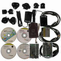
Manufacturer Part Number
1321XDSK-BDM
Description
KIT STARTER DEV 1321X W/USB
Manufacturer
Freescale Semiconductor
Type
Sensor Demor
Specifications of 1321XDSK-BDM
Frequency
2.4GHz
Wireless Frequency
2.4 GHz
Interface Type
SPI
Modulation
DSSS OQPSK
Security
128 bit AES
Operating Voltage
2 VDC to 3.4 VDC
Output Power
2 dBm
Antenna
F-Antenna
Operating Temperature Range
- 40 C to + 85 C
For Use With/related Products
MC1321x
Lead Free Status / RoHS Status
Contains lead / RoHS compliant by exemption


5.4
The ICG provides multiple options for MCU clock sources. This block along with the ability to provide
the MCU clock form the modem offers a user great flexibility when making choices between cost,
precision, current draw, and performance. As seen in
The module is intended to be very user friendly with many of the features occurring automatically without
user intervention.
5.4.1
Features of the ICG and clock distribution system:
Freescale Semiconductor
•
•
•
•
•
•
•
Oscillator Block — The Oscillator Block provides means for connecting an external crystal or
resonator. Two frequency ranges are software selectable to allow optimal start-up and stability.
Alternatively, the oscillator block can be used to route an external square wave to the MCU system
clock. External sources such as the modem CLKO output can provide a low cost source or a very
precise clock source. The oscillator is capable of being configured for low power mode or high
amplitude mode as selected by HGO.
Internal Reference Generator — The Internal Reference Generator consists of two controlled
clock sources. One is designed to be approximately 8 MHz and can be selected as a local clock for
the background debug controller. The other internal reference clock source is typically 243 kHz
and can be trimmed for finer accuracy via software when a precise timed event is input to the MCU.
This provides a highly reliable, low-cost clock source.
Frequency-Locked Loop — A Frequency-Locked Loop (FLL) stage takes either the internal or
external clock source and multiplies it to a higher frequency. Status bits provide information when
the circuit has achieved lock and when it falls out of lock. Additionally, this block can monitor the
external reference clock and signals whether the clock is valid or not.
Clock Select Block — The Clock Select Block provides several switch options for connecting
different clock sources to the system clock tree. ICGDCLK is the multiplied clock frequency out
of the FLL, ICGERCLK is the reference clock frequency from the crystal or external clock source,
and FFE (fixed frequency enable) is a control signal used to control the system fixed frequency
clock (XCLK). ICGLCLK is the clock source for the background debug controller (BDC).
Several options for the MCU primary clock source allow a wide range of cost, frequency, and
precision choices:
— 32 kHz–100 kHz crystal or resonator
— 1 MHz–16 MHz crystal or resonator
— External clock supplied by modem CLKO or other source
— Internal reference generator
Defaults to self-clocked mode to minimize startup delays
Frequency-locked loop (FLL) generates 8 MHz to 40 MHz (for bus rates up to 20 MHz). When
using modem CLKO as external source, maximum FLL frequency is 32 MHz (16 MHz bus rate)
with CLKO = 16 MHz or maximum FLL frequency is 40 MHz (20 MHz bus rate) with CLKO =
4 MHz.
MCU Internal Clock Generator (ICG)
Features
MC13211/212/213 Technical Data, Rev. 1.8
Figure
17, the ICG consists of four functional blocks.
29
Related parts for 1321XDSK-BDM
Image
Part Number
Description
Manufacturer
Datasheet
Request
R

Part Number:
Description:
KIT STARTER DEVELOPER 1321X
Manufacturer:
Freescale Semiconductor
Datasheet:

Part Number:
Description:
Manufacturer:
Freescale Semiconductor, Inc
Datasheet:
Part Number:
Description:
Manufacturer:
Freescale Semiconductor, Inc
Datasheet:
Part Number:
Description:
Manufacturer:
Freescale Semiconductor, Inc
Datasheet:
Part Number:
Description:
Manufacturer:
Freescale Semiconductor, Inc
Datasheet:
Part Number:
Description:
Manufacturer:
Freescale Semiconductor, Inc
Datasheet:
Part Number:
Description:
Manufacturer:
Freescale Semiconductor, Inc
Datasheet:
Part Number:
Description:
Manufacturer:
Freescale Semiconductor, Inc
Datasheet:
Part Number:
Description:
Manufacturer:
Freescale Semiconductor, Inc
Datasheet:
Part Number:
Description:
Manufacturer:
Freescale Semiconductor, Inc
Datasheet:
Part Number:
Description:
Manufacturer:
Freescale Semiconductor, Inc
Datasheet:
Part Number:
Description:
Manufacturer:
Freescale Semiconductor, Inc
Datasheet:
Part Number:
Description:
Manufacturer:
Freescale Semiconductor, Inc
Datasheet:
Part Number:
Description:
Manufacturer:
Freescale Semiconductor, Inc
Datasheet:
Part Number:
Description:
Manufacturer:
Freescale Semiconductor, Inc
Datasheet: