1321XDSK-BDM Freescale Semiconductor, 1321XDSK-BDM Datasheet - Page 51
1321XDSK-BDM
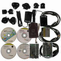
Manufacturer Part Number
1321XDSK-BDM
Description
KIT STARTER DEV 1321X W/USB
Manufacturer
Freescale Semiconductor
Type
Sensor Demor
Specifications of 1321XDSK-BDM
Frequency
2.4GHz
Wireless Frequency
2.4 GHz
Interface Type
SPI
Modulation
DSSS OQPSK
Security
128 bit AES
Operating Voltage
2 VDC to 3.4 VDC
Output Power
2 dBm
Antenna
F-Antenna
Operating Temperature Range
- 40 C to + 85 C
For Use With/related Products
MC1321x
Lead Free Status / RoHS Status
Contains lead / RoHS compliant by exemption


1
2
3
4
5
6
Freescale Semiconductor
Input low voltage (V
Input low voltage (1.8 V ≤ V
Input hysteresis (all digital inputs)
Input leakage current (per pin)
High impedance (off-state) leakage current (per pin)
Internal pullup and pulldown resistors
Internal pulldown resistors (Port A4–A7 and IRQ)
Output high voltage (V
Output high voltage (ports C and F)
Maximum total I
Output low voltage (V
Output low voltage (ports C and F)
Maximum total I
dc injection current
Input capacitance (all non-supply pins)
Typicals are measured at 25°C.
This parameter is characterized and not tested on each device.
Measurement condition for pull resistors: V
Power supply must maintain regulation within operating V
conditions. If positive injection current (V
in external power supply going out of regulation. Ensure external V
current. This will be the greatest risk when the MCU is not consuming power. Examples are: if no system clock is present, or if
clock rate is very low which would reduce overall power consumption.
All functional non-supply pins are internally clamped to V
Input must be current limited to the value specified. To determine the value of the required current-limiting resistor, calculate
resistance values for positive and negative clamp voltages, then use the larger of the two values.
(all digital inputs)
(all port pins and IRQ)
I
I
I
I
I
I
Single pin limit
Total MCU limit, includes sum of all stressed pins
I
OH
OH
OH
OL
OL
OL
V
V
I
OL
OH
In
In
V
= 2.0 mA (ports A, B, D, E, and G)
= 6 mA (V
= 3 mA (V
= –10 mA (V
= –6 mA (V
= –3 mA (V
= 10.0 mA (V
= V
= V
= –2 mA (ports A, B, D, E, and G)
IN
< V
DD
DD
or V
or V
SS
OH
OL
DD
DD
, V
SS
SS,
DD
DD
for all port pins
IN
DD
for all port pins
≥ 2.3 V)
≥ 1.8 V)
DD
, all input/output
4, 5, 6, 7, 8
DD
all input only pins
≥ 2.3 V)
≥ 1.8 V)
> V
DD
≥ 2.7 V)
DD
≥ 2.7 V)
> 2.3 V) (all digital inputs)
≥ 1.8 V)
DD
≥ 1.8 V)
DD
Parameter
≤ 2.3 V)
Table 12. MCU DC Characteristics (continued)
(Temperature Range = –40 to 85°C Ambient)
3
(2)
MC13211/212/213 Technical Data, Rev. 1.8
In
> V
In
= V
DD
) is greater than I
SS
for pullup and V
SS
DD
and V
range during instantaneous and operating maximum current
DD
DD
DD
In
, the injection current may flow out of V
Symbol
.
|I
= V
V
load will shunt current greater than maximum injection
|I
R
R
V
V
I
|I
|I
OHT
C
V
V
OLT
OZ
hys
OH
IC
In
PU
PD
OL
IL
IL
In
DD
|
|
|
|
for pulldown.
0.06 × V
V
V
DD
DD
17.5
17.5
Min
—
—
—
—
—
—
—
—
—
—
—
—
—
– 0.5
– 0.5
DD
Typical
0.025
0.025
1
0.35 × V
0.30 × V
DD
Max
52.5
52.5
1.0
1.0
0.5
0.5
0.5
0.5
0.2
—
—
—
—
—
60
60
5
7
and could result
DD
DD
kohm
kohm
Unit
mA
mA
mA
mA
μA
μA
pF
V
V
V
V
V
51
Related parts for 1321XDSK-BDM
Image
Part Number
Description
Manufacturer
Datasheet
Request
R

Part Number:
Description:
KIT STARTER DEVELOPER 1321X
Manufacturer:
Freescale Semiconductor
Datasheet:

Part Number:
Description:
Manufacturer:
Freescale Semiconductor, Inc
Datasheet:
Part Number:
Description:
Manufacturer:
Freescale Semiconductor, Inc
Datasheet:
Part Number:
Description:
Manufacturer:
Freescale Semiconductor, Inc
Datasheet:
Part Number:
Description:
Manufacturer:
Freescale Semiconductor, Inc
Datasheet:
Part Number:
Description:
Manufacturer:
Freescale Semiconductor, Inc
Datasheet:
Part Number:
Description:
Manufacturer:
Freescale Semiconductor, Inc
Datasheet:
Part Number:
Description:
Manufacturer:
Freescale Semiconductor, Inc
Datasheet:
Part Number:
Description:
Manufacturer:
Freescale Semiconductor, Inc
Datasheet:
Part Number:
Description:
Manufacturer:
Freescale Semiconductor, Inc
Datasheet:
Part Number:
Description:
Manufacturer:
Freescale Semiconductor, Inc
Datasheet:
Part Number:
Description:
Manufacturer:
Freescale Semiconductor, Inc
Datasheet:
Part Number:
Description:
Manufacturer:
Freescale Semiconductor, Inc
Datasheet:
Part Number:
Description:
Manufacturer:
Freescale Semiconductor, Inc
Datasheet:
Part Number:
Description:
Manufacturer:
Freescale Semiconductor, Inc
Datasheet: