1321XDSK-BDM Freescale Semiconductor, 1321XDSK-BDM Datasheet - Page 46
1321XDSK-BDM
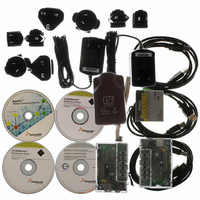
Manufacturer Part Number
1321XDSK-BDM
Description
KIT STARTER DEV 1321X W/USB
Manufacturer
Freescale Semiconductor
Type
Sensor Demor
Specifications of 1321XDSK-BDM
Frequency
2.4GHz
Wireless Frequency
2.4 GHz
Interface Type
SPI
Modulation
DSSS OQPSK
Security
128 bit AES
Operating Voltage
2 VDC to 3.4 VDC
Output Power
2 dBm
Antenna
F-Antenna
Operating Temperature Range
- 40 C to + 85 C
For Use With/related Products
MC1321x
Lead Free Status / RoHS Status
Contains lead / RoHS compliant by exemption


6
This section details maximum ratings for the 71 pin LGA package and recommended operating conditions,
DC characteristics, and AC characteristics for the modem, and the MCU.
6.1
Absolute maximum ratings are stress ratings only, and functional operation at the maximum rating is not
guaranteed. Stress beyond the limits specified in
damage to the device. For functional operating conditions, refer to the remaining tables in this section.
This device contains circuitry protecting against damage due to high static voltage or electrical fields;
however, it is advised that normal precautions be taken to avoid application of any voltages higher than
maximum-rated voltages to this high-impedance circuit. Reliability of operation is enhanced if unused
inputs are tied to an appropriate logic voltage level (for instance, either V
pull-up resistor associated with the pin is enabled.
Table 6
46
Maximum Junction Temperature
Storage Temperature Range
Power Supply Voltage
Digital Input Voltage
RF Input Power
Maximum Current into V
Instantaneous Maximum Current (Single Pin Limit)
Note: Maximum Ratings are those values beyond which damage to the device may occur.
Note: Meets Human Body Model (HBM) = 2 kV. RF input/output pins have no ESD protection.
Functional operation should be restricted to the limits in the Electrical Characteristics
or Recommended Operating Conditions tables.
— A-only
— A OR B
— A then B
— A AND B data (full mode)
— A AND NOT B data (full mode)
— Event-only B (store data)
— A then event-only B (store data)
— Inside range (A ≤ address ≤ B)
— Outside range (address < A or address > B)
System Electrical Specification
shows the maximum ratings for the 71 Pin LGA package.
SiP LGA Package Maximum Ratings
DD
Rating
Table 6. LGA Package Maximum Ratings
MC13211/212/213 Technical Data, Rev. 1.8
1
,
2
,
3
Table 6
may affect device reliability or cause permanent
V
BATT
Symbol
P
T
Vin
I
T
, V
DD
max
I
stg
D
J
DDINT
SS
or V
-0.3 to (V
DD
-55 to 125
-0.3 to 3.6
) or the programmable
Value
± 25
125
120
DDINT
10
Freescale Semiconductor
+ 0.3)
dBm
Unit
Vdc
mA
mA
°C
°C
Related parts for 1321XDSK-BDM
Image
Part Number
Description
Manufacturer
Datasheet
Request
R

Part Number:
Description:
KIT STARTER DEVELOPER 1321X
Manufacturer:
Freescale Semiconductor
Datasheet:

Part Number:
Description:
Manufacturer:
Freescale Semiconductor, Inc
Datasheet:
Part Number:
Description:
Manufacturer:
Freescale Semiconductor, Inc
Datasheet:
Part Number:
Description:
Manufacturer:
Freescale Semiconductor, Inc
Datasheet:
Part Number:
Description:
Manufacturer:
Freescale Semiconductor, Inc
Datasheet:
Part Number:
Description:
Manufacturer:
Freescale Semiconductor, Inc
Datasheet:
Part Number:
Description:
Manufacturer:
Freescale Semiconductor, Inc
Datasheet:
Part Number:
Description:
Manufacturer:
Freescale Semiconductor, Inc
Datasheet:
Part Number:
Description:
Manufacturer:
Freescale Semiconductor, Inc
Datasheet:
Part Number:
Description:
Manufacturer:
Freescale Semiconductor, Inc
Datasheet:
Part Number:
Description:
Manufacturer:
Freescale Semiconductor, Inc
Datasheet:
Part Number:
Description:
Manufacturer:
Freescale Semiconductor, Inc
Datasheet:
Part Number:
Description:
Manufacturer:
Freescale Semiconductor, Inc
Datasheet:
Part Number:
Description:
Manufacturer:
Freescale Semiconductor, Inc
Datasheet:
Part Number:
Description:
Manufacturer:
Freescale Semiconductor, Inc
Datasheet: