1321XDSK-BDM Freescale Semiconductor, 1321XDSK-BDM Datasheet - Page 33
1321XDSK-BDM
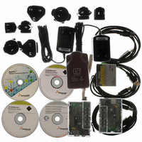
Manufacturer Part Number
1321XDSK-BDM
Description
KIT STARTER DEV 1321X W/USB
Manufacturer
Freescale Semiconductor
Type
Sensor Demor
Specifications of 1321XDSK-BDM
Frequency
2.4GHz
Wireless Frequency
2.4 GHz
Interface Type
SPI
Modulation
DSSS OQPSK
Security
128 bit AES
Operating Voltage
2 VDC to 3.4 VDC
Output Power
2 dBm
Antenna
F-Antenna
Operating Temperature Range
- 40 C to + 85 C
For Use With/related Products
MC1321x
Lead Free Status / RoHS Status
Contains lead / RoHS compliant by exemption


5.6
The MC1321x HCS08 has seven I/O ports which include a total of 56 general-purpose I/O signals (one of
these pins, PTG0, is output only). The MC1321x family does not use all the these signals as denoted in
Figure
as pinned-out I/O or as internally dedicated signal for communication with the 802.15.4 modem.
As stated above port F and part of port G are not utilized. These signals and any unused IO should be
programmed as outputs during initialization for lowest power operation. Many of these pins are shared
with on-chip peripherals such as timer systems, various communication ports, or keyboard interrupts.
When these other modules are not controlling the port pins, they revert to general-purpose I/O control. For
each I/O pin, a port data bit provides access to input (read) and output (write) data, a data direction bit
controls the direction of the pin, and a pullup enable bit enables an internal pullup device (provided the pin
is configured as an input), and a slew rate control bit controls the rise and fall times of the pins.Parallel I/O
features include:
5.7
5.7.1
The HCS08 provides one serial peripheral interface (SPI) module which is connected within the SiP to the
modem SPI port. The four pins associated with SPI functionality are shared with port E pins 2–5. When
the SPI is enabled, the direction of pins is controlled by module configuration.
The MCU SPI port is used only in master mode on the MC1321x family. The user must program the SPI
module for the proper characteristics as listed in the features below and also program the SS signal to have
the proper use to support the modem transaction protocol for the modem CE signal.
Freescale Semiconductor
•
•
•
•
•
•
•
•
•
•
•
15. Port F and part of port G are not utilized. The MC1321x family makes use of the remaining I/O
A total of 32 general-purpose I/O pins in seven ports (PTG0 is output only)
High-current drivers on port C
Hysteresis input buffers
Software-controlled pullups on each input pin
Software-controlled slew rate output buffers
Eight port A pins shared with KBI1
Eight port B pins shared with ATD1
Eight high-current port C pins shared with SCI2 and IIC1
Eight port D pins shared with TPM1 and TPM2
Eight port E pins shared with SCI1 and SPI1
Eight port G pins shared with EXTAL, XTAL, and BKGD/MS
Parallel Input/Output
MCU Peripherals
Modem Dedicated Serial Peripheral Interface (SPI) Module
Not all port G signals and no port F signals are bonded out, but are present
in the MCU hardware (see
programmed as outputs set to the low state.
MC13211/212/213 Technical Data, Rev. 1.8
Figure
NOTE
15). These port I/O signals should be
33
Related parts for 1321XDSK-BDM
Image
Part Number
Description
Manufacturer
Datasheet
Request
R

Part Number:
Description:
KIT STARTER DEVELOPER 1321X
Manufacturer:
Freescale Semiconductor
Datasheet:

Part Number:
Description:
Manufacturer:
Freescale Semiconductor, Inc
Datasheet:
Part Number:
Description:
Manufacturer:
Freescale Semiconductor, Inc
Datasheet:
Part Number:
Description:
Manufacturer:
Freescale Semiconductor, Inc
Datasheet:
Part Number:
Description:
Manufacturer:
Freescale Semiconductor, Inc
Datasheet:
Part Number:
Description:
Manufacturer:
Freescale Semiconductor, Inc
Datasheet:
Part Number:
Description:
Manufacturer:
Freescale Semiconductor, Inc
Datasheet:
Part Number:
Description:
Manufacturer:
Freescale Semiconductor, Inc
Datasheet:
Part Number:
Description:
Manufacturer:
Freescale Semiconductor, Inc
Datasheet:
Part Number:
Description:
Manufacturer:
Freescale Semiconductor, Inc
Datasheet:
Part Number:
Description:
Manufacturer:
Freescale Semiconductor, Inc
Datasheet:
Part Number:
Description:
Manufacturer:
Freescale Semiconductor, Inc
Datasheet:
Part Number:
Description:
Manufacturer:
Freescale Semiconductor, Inc
Datasheet:
Part Number:
Description:
Manufacturer:
Freescale Semiconductor, Inc
Datasheet:
Part Number:
Description:
Manufacturer:
Freescale Semiconductor, Inc
Datasheet: