1321XDSK-BDM Freescale Semiconductor, 1321XDSK-BDM Datasheet - Page 21
1321XDSK-BDM
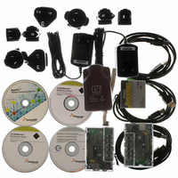
Manufacturer Part Number
1321XDSK-BDM
Description
KIT STARTER DEV 1321X W/USB
Manufacturer
Freescale Semiconductor
Type
Sensor Demor
Specifications of 1321XDSK-BDM
Frequency
2.4GHz
Wireless Frequency
2.4 GHz
Interface Type
SPI
Modulation
DSSS OQPSK
Security
128 bit AES
Operating Voltage
2 VDC to 3.4 VDC
Output Power
2 dBm
Antenna
F-Antenna
Operating Temperature Range
- 40 C to + 85 C
For Use With/related Products
MC1321x
Lead Free Status / RoHS Status
Contains lead / RoHS compliant by exemption


4.6.2.2
Although the SPI port of the MCU transfers data in bursts of 8 bits, the 802.15.4 modem requires that a
complete SPI transaction be framed by CE, and there will be three (3) or more bursts per transaction. The
assertion of CE to low signals the start of a transaction. The first SPI burst is a write of an 8-bit header to
the transceiver (MOSI is valid) that defines a 6-bit address of the internal resource being accessed and
identifies the access as being a read or write operation. In this context, a write is data written to the 802.15.4
modem and a read is data written to the SPI master. The following SPI bursts will be either the write data
(MOSI is valid) to the transceiver or read data from the transceiver (MISO is valid).
Although the SPI bus is capable of sending data simultaneously between master and slave, the 802.15.4
modem never uses this mode. The number of data bytes (payload) will be a minimum of 2 bytes and can
extend to a larger number depending on the type of access. After the final SPI burst, CE is negated to high
to signal the end of the transaction.
An example SPI read transaction with a 2-byte payload is shown in
Freescale Semiconductor
SPI Transaction Operation
SPICLK
CE
MISO
MOSI
Clock Burst
Figure 11. SPI Read Transaction Diagram
MC13211/212/213 Technical Data, Rev. 1.8
Header
Valid
Valid
Read data
Figure
Valid
11.
21
Related parts for 1321XDSK-BDM
Image
Part Number
Description
Manufacturer
Datasheet
Request
R

Part Number:
Description:
KIT STARTER DEVELOPER 1321X
Manufacturer:
Freescale Semiconductor
Datasheet:

Part Number:
Description:
Manufacturer:
Freescale Semiconductor, Inc
Datasheet:
Part Number:
Description:
Manufacturer:
Freescale Semiconductor, Inc
Datasheet:
Part Number:
Description:
Manufacturer:
Freescale Semiconductor, Inc
Datasheet:
Part Number:
Description:
Manufacturer:
Freescale Semiconductor, Inc
Datasheet:
Part Number:
Description:
Manufacturer:
Freescale Semiconductor, Inc
Datasheet:
Part Number:
Description:
Manufacturer:
Freescale Semiconductor, Inc
Datasheet:
Part Number:
Description:
Manufacturer:
Freescale Semiconductor, Inc
Datasheet:
Part Number:
Description:
Manufacturer:
Freescale Semiconductor, Inc
Datasheet:
Part Number:
Description:
Manufacturer:
Freescale Semiconductor, Inc
Datasheet:
Part Number:
Description:
Manufacturer:
Freescale Semiconductor, Inc
Datasheet:
Part Number:
Description:
Manufacturer:
Freescale Semiconductor, Inc
Datasheet:
Part Number:
Description:
Manufacturer:
Freescale Semiconductor, Inc
Datasheet:
Part Number:
Description:
Manufacturer:
Freescale Semiconductor, Inc
Datasheet:
Part Number:
Description:
Manufacturer:
Freescale Semiconductor, Inc
Datasheet: