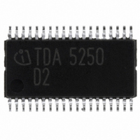
TDA5250 Infineon Technologies, TDA5250 Datasheet - Page 32

TDA5250
Manufacturer Part Number
TDA5250
Description
TX/RX ASK/FSK 868-870MHZ 38TSSOP
Manufacturer
Infineon Technologies
Type
Transceiverr
Specifications of TDA5250
Package / Case
38-TSSOP
Frequency
868MHz
Data Rate - Maximum
64kbps
Modulation Or Protocol
ASK, FSK
Applications
RKE, Remote Control Systems
Power - Output
9dBm
Sensitivity
-109dBm
Voltage - Supply
2.1 V ~ 5.5 V
Current - Receiving
9mA
Current - Transmitting
12mA
Data Interface
PCB, Surface Mount
Antenna Connector
PCB, Surface Mount
Operating Temperature
-40°C ~ 85°C
Operating Frequency
870 MHz
Operating Supply Voltage
2.5 V, 3.3 V, 5 V
Maximum Operating Temperature
+ 85 C
Minimum Operating Temperature
- 40 C
Mounting Style
SMD/SMT
Operating Temperature (min)
-40C
Operating Temperature (max)
85C
Operating Temperature Classification
Industrial
Product Depth (mm)
4.4mm
Product Length (mm)
9.7mm
Operating Supply Voltage (min)
2.1V
Operating Supply Voltage (max)
5.5V
Lead Free Status / RoHS Status
Lead free / RoHS Compliant
Memory Size
-
Lead Free Status / Rohs Status
Compliant
Other names
SP000012956
TDA5250
TDA5250INTR
TDA5250XT
TDA5250XT
TDA5250
TDA5250INTR
TDA5250XT
TDA5250XT
Available stocks
Company
Part Number
Manufacturer
Quantity
Price
Company:
Part Number:
TDA5250
Manufacturer:
Infineon Technologies
Quantity:
135
Company:
Part Number:
TDA5250D2
Manufacturer:
INFINEON
Quantity:
300
Part Number:
TDA5250D2
Manufacturer:
INFINEON/英飞凌
Quantity:
20 000
2.4.16
Figure 2-9
Table 2-31
SLAVE MODE: The receive and transmit operation is fully controlled by an external control device
via the respective RxTx, AskFsk, PwdDD, and Data pins. The wakeup logic is inactive in this case.
After RESET or 1
CONFIG register the mode may be changed.
SELF POLLING MODE: The chip turns itself on periodically to receive using a built-in 32kHz RC
oscillator. The timing of this is determined by the ON_TIME and OFF_TIME registers, the duty cycle
can be set between 0 and 100% in 31.25µs increments. The data detect logic is enabled and a 15µs
LOW impulse is provided at PwdDD pin (Pin 27), if the received data is valid.
Figure 2-10
Data Sheet
MODE_1
SELF POLLING MODE
0
0
1
Wakeup Logic
MODE settings: CONFIG register
PwdDD pin in
Wakeup Logic States
Timing for Self Polling Mode (ADC & Data Detect in one shot mode)
st
Power-up the chip is in SLAVE MODE. By setting MODE_1 and MODE_2 in the
Action
SELF POLLING
MODE_1 = 1
MODE_2 = X
MODE_2
MODE
X
0
1
min. 2.6ms
RX ON: valid Data
ON_TIME
SLAVE MODE
MODE_1 = 0
MODE_2 = 0
(default)
15µs
32
OFF_TIME
TIMER MODE
SELF POLLING MODE
MODE_1 = 0
MODE_2 = 1
SLAVE MODE
TIMER MODE
Mode
RX ON: invalid Data
ON_TIME
Functional Description
TDA5250 D2
Version 1.7
timing_selfpllmode.wmf
2007-02-26
t
3_modes.wmf
t


