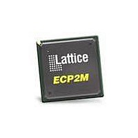
LFE2-20E-5FN484C Lattice, LFE2-20E-5FN484C Datasheet - Page 106

LFE2-20E-5FN484C
Manufacturer Part Number
LFE2-20E-5FN484C
Description
FPGA - Field Programmable Gate Array 21K LUTs 331 I/O DSP 1.2V -5
Manufacturer
Lattice
Series
LatticeECP2r
Datasheet
1.LFE2-12SE-6FN256C.pdf
(389 pages)
Specifications of LFE2-20E-5FN484C
Number Of Macrocells
21000
Number Of Programmable I/os
331
Data Ram Size
282624
Supply Voltage (max)
1.26 V
Maximum Operating Temperature
+ 85 C
Minimum Operating Temperature
0 C
Mounting Style
SMD/SMT
Supply Voltage (min)
1.14 V
Package / Case
FPBGA-484
No. Of Logic Blocks
21000
No. Of Macrocells
10500
No. Of Speed Grades
5
Total Ram Bits
276Kbit
No. Of I/o's
331
Clock Management
DLL, PLL
I/o Supply Voltage
3.465V
Rohs Compliant
Yes
Lead Free Status / RoHS Status
Lead free / RoHS Compliant
Available stocks
Company
Part Number
Manufacturer
Quantity
Price
Company:
Part Number:
LFE2-20E-5FN484C
Manufacturer:
Lattice
Quantity:
135
Company:
Part Number:
LFE2-20E-5FN484C
Manufacturer:
TI
Quantity:
2 658
Company:
Part Number:
LFE2-20E-5FN484C
Manufacturer:
Lattice Semiconductor Corporation
Quantity:
10 000
Part Number:
LFE2-20E-5FN484C
Manufacturer:
LATTICE
Quantity:
20 000
- Current page: 106 of 389
- Download datasheet (5Mb)
Signal Descriptions (Cont.)
Lattice Semiconductor
[LOC]_SQ_VCCIBm
[LOC]_SQ_VCCOBm
[LOC]_SQ_HDOUTNm
[LOC]_SQ_HDOUTPm
[LOC]_SQ_HDINNm
[LOC]_SQ_HDINPm
[LOC]_SQ_VCCTXm
[LOC]_SQ_VCCRXm
1. These signals are relevant for LatticeECP2M family.
2. m defines the associated channel in the Quad.
3. These signals are defined in Quads [LOC] indicates the corner SERDES Quad is located: ULC (upper left), URC (upper right), LLC (lower
4. When placing switching I/Os around these critical pins that are designed to supply the device with the proper reference or supply voltage,
5. There may be SPLLs that do not have dedicated I/Os.
left), LRC (lower right).
care must be given. For more information, refer to TN1159,
Signal Name
4
4
I/O
—
—
—
—
O
O
I
I
Input buffer power supply, channel m (1.2V/1.5V). This pin should be left float-
ing if the channel is unused.
Output buffer power supply, channel m (1.2V/1.5V). This pin should be left
floating if the channel is unused.
High-speed output, negative channel m
High-speed output, positive channel m
High-speed input, negative channel m
High-speed input, positive channel m
Transmitter power supply, channel m (1.2V). This pin must be tied to 1.2V
even if the channel is unused.
Receiver power supply, channel m (1.2V). This pin must be tied to 1.2V even if
the channel is unused.
LatticeECP2/M Pin Assignment
4-3
LatticeECP2/M Family Data Sheet
Description
Recommendations.
Pinout Information
Related parts for LFE2-20E-5FN484C
Image
Part Number
Description
Manufacturer
Datasheet
Request
R

Part Number:
Description:
IC, LATTICEECP2 FPGA, 420MHZ, QFP-208
Manufacturer:
LATTICE SEMICONDUCTOR
Datasheet:

Part Number:
Description:
FPGA - Field Programmable Gate Array 21K LUTs 331 I/O DSP 1.2V -5
Manufacturer:
Lattice

Part Number:
Description:
FPGA - Field Programmable Gate Array 21K LUTs 402 I/O DSP 1.2V -5
Manufacturer:
Lattice

Part Number:
Description:
FPGA - Field Programmable Gate Array 21K LUTs 193 I/O DSP 1.2V -5 I
Manufacturer:
Lattice

Part Number:
Description:
FPGA - Field Programmable Gate Array 21K LUTs 402 I/O DSP 1.2V -5 I
Manufacturer:
Lattice

Part Number:
Description:
FPGA - Field Programmable Gate Array 21K LUTs 131 I/O DSP 1.2V -5
Manufacturer:
Lattice

Part Number:
Description:
FPGA - Field Programmable Gate Array 21K LUTs 131 I/O DSP 1.2V -5 I
Manufacturer:
Lattice

Part Number:
Description:
IC FPGA 21KLUTS 193I/O 256FPBGA
Manufacturer:
Lattice
Datasheet:
Part Number:
Description:
IC, LATTICEECP2 FPGA, 420MHZ, FPBGA-672
Manufacturer:
LATTICE SEMICONDUCTOR
Datasheet:

Part Number:
Description:
IC, LATTICEECP2 FPGA, 420MHZ, QFP-208
Manufacturer:
LATTICE SEMICONDUCTOR
Datasheet:
Part Number:
Description:
FPGA LatticeECP2 Family 21000 Cells 90nm (CMOS) Technology 1.2V 256-Pin FBGA
Manufacturer:
LATTICE SEMICONDUCTOR
Datasheet:
Part Number:
Description:
FPGA LatticeECP2 Family 21000 Cells 90nm (CMOS) Technology 1.2V 484-Pin FBGA
Manufacturer:
LATTICE SEMICONDUCTOR
Datasheet:
Part Number:
Description:
FPGA LatticeECP2 Family 21000 Cells 90nm (CMOS) Technology 1.2V 484-Pin FBGA
Manufacturer:
LATTICE SEMICONDUCTOR
Datasheet:
Part Number:
Description:
FPGA LatticeECP2 Family 21000 Cells 90nm (CMOS) Technology 1.2V 484-Pin FBGA
Manufacturer:
LATTICE SEMICONDUCTOR
Datasheet:
Part Number:
Description:
FPGA LatticeECP2 Family 21000 Cells 90nm (CMOS) Technology 1.2V 484-Pin FBGA
Manufacturer:
LATTICE SEMICONDUCTOR
Datasheet:


