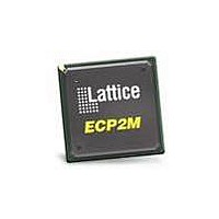
LFE2-20E-5FN484C Lattice, LFE2-20E-5FN484C Datasheet - Page 27

LFE2-20E-5FN484C
Manufacturer Part Number
LFE2-20E-5FN484C
Description
FPGA - Field Programmable Gate Array 21K LUTs 331 I/O DSP 1.2V -5
Manufacturer
Lattice
Series
LatticeECP2r
Datasheet
1.LFE2-12SE-6FN256C.pdf
(389 pages)
Specifications of LFE2-20E-5FN484C
Number Of Macrocells
21000
Number Of Programmable I/os
331
Data Ram Size
282624
Supply Voltage (max)
1.26 V
Maximum Operating Temperature
+ 85 C
Minimum Operating Temperature
0 C
Mounting Style
SMD/SMT
Supply Voltage (min)
1.14 V
Package / Case
FPBGA-484
No. Of Logic Blocks
21000
No. Of Macrocells
10500
No. Of Speed Grades
5
Total Ram Bits
276Kbit
No. Of I/o's
331
Clock Management
DLL, PLL
I/o Supply Voltage
3.465V
Rohs Compliant
Yes
Lead Free Status / RoHS Status
Lead free / RoHS Compliant
Available stocks
Company
Part Number
Manufacturer
Quantity
Price
Company:
Part Number:
LFE2-20E-5FN484C
Manufacturer:
Lattice
Quantity:
135
Company:
Part Number:
LFE2-20E-5FN484C
Manufacturer:
TI
Quantity:
2 658
Company:
Part Number:
LFE2-20E-5FN484C
Manufacturer:
Lattice Semiconductor Corporation
Quantity:
10 000
Part Number:
LFE2-20E-5FN484C
Manufacturer:
LATTICE
Quantity:
20 000
- Current page: 27 of 389
- Download datasheet (5Mb)
Lattice Semiconductor
MAC sysDSP Element
In this case, the two operands, A and B, are multiplied and the result is added with the previous accumulated value.
This accumulated value is available at the output. The user can enable the input and pipeline registers, but the out-
put register is always enabled. The output register is used to store the accumulated value. The Accumulators in the
DSP blocks in the LatticeECP2/M family can be initialized dynamically. A registered overflow signal is also avail-
able. The overflow conditions are provided later in this document. Figure 2-24 shows the MAC sysDSP element.
Figure 2-24. MAC sysDSP
Multiplicand
Multiplier
Signed A
Signed B
Addn
Accumsload
Serial Register B in
n
Input Data
Register B
n
n
SROB
n
Register
Register
Register
Register
Input
Input
Input
Input
m
Input Data
Register A
m
n
SROA
Serial Register A in
m
Register
Register
Register
Register
Pipeline
Pipeline
Pipeline
Pipeline
m
n
2-24
To Accumulator
To Accumulator
To Accumulator
To Accumulator
Multiplier
Register
Pipeline
x
(default)
m+n
Accumulator
LatticeECP2/M Family Data Sheet
CLK (CLK0,CLK1,CLK2,CLK3)
RST(RST0,RST1,RST2,RST3)
CE (CE0,CE1,CE2,CE3)
m+n+16
(default)
Preload
(default)
m+n+16
Architecture
Output
Overflow
signal
Related parts for LFE2-20E-5FN484C
Image
Part Number
Description
Manufacturer
Datasheet
Request
R

Part Number:
Description:
IC, LATTICEECP2 FPGA, 420MHZ, QFP-208
Manufacturer:
LATTICE SEMICONDUCTOR
Datasheet:

Part Number:
Description:
FPGA - Field Programmable Gate Array 21K LUTs 331 I/O DSP 1.2V -5
Manufacturer:
Lattice

Part Number:
Description:
FPGA - Field Programmable Gate Array 21K LUTs 402 I/O DSP 1.2V -5
Manufacturer:
Lattice

Part Number:
Description:
FPGA - Field Programmable Gate Array 21K LUTs 193 I/O DSP 1.2V -5 I
Manufacturer:
Lattice

Part Number:
Description:
FPGA - Field Programmable Gate Array 21K LUTs 402 I/O DSP 1.2V -5 I
Manufacturer:
Lattice

Part Number:
Description:
FPGA - Field Programmable Gate Array 21K LUTs 131 I/O DSP 1.2V -5
Manufacturer:
Lattice

Part Number:
Description:
FPGA - Field Programmable Gate Array 21K LUTs 131 I/O DSP 1.2V -5 I
Manufacturer:
Lattice

Part Number:
Description:
IC FPGA 21KLUTS 193I/O 256FPBGA
Manufacturer:
Lattice
Datasheet:
Part Number:
Description:
IC, LATTICEECP2 FPGA, 420MHZ, FPBGA-672
Manufacturer:
LATTICE SEMICONDUCTOR
Datasheet:

Part Number:
Description:
IC, LATTICEECP2 FPGA, 420MHZ, QFP-208
Manufacturer:
LATTICE SEMICONDUCTOR
Datasheet:
Part Number:
Description:
FPGA LatticeECP2 Family 21000 Cells 90nm (CMOS) Technology 1.2V 256-Pin FBGA
Manufacturer:
LATTICE SEMICONDUCTOR
Datasheet:
Part Number:
Description:
FPGA LatticeECP2 Family 21000 Cells 90nm (CMOS) Technology 1.2V 484-Pin FBGA
Manufacturer:
LATTICE SEMICONDUCTOR
Datasheet:
Part Number:
Description:
FPGA LatticeECP2 Family 21000 Cells 90nm (CMOS) Technology 1.2V 484-Pin FBGA
Manufacturer:
LATTICE SEMICONDUCTOR
Datasheet:
Part Number:
Description:
FPGA LatticeECP2 Family 21000 Cells 90nm (CMOS) Technology 1.2V 484-Pin FBGA
Manufacturer:
LATTICE SEMICONDUCTOR
Datasheet:
Part Number:
Description:
FPGA LatticeECP2 Family 21000 Cells 90nm (CMOS) Technology 1.2V 484-Pin FBGA
Manufacturer:
LATTICE SEMICONDUCTOR
Datasheet:


