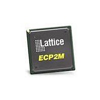
LFE2-20E-5FN484C Lattice, LFE2-20E-5FN484C Datasheet - Page 24

LFE2-20E-5FN484C
Manufacturer Part Number
LFE2-20E-5FN484C
Description
FPGA - Field Programmable Gate Array 21K LUTs 331 I/O DSP 1.2V -5
Manufacturer
Lattice
Series
LatticeECP2r
Datasheet
1.LFE2-12SE-6FN256C.pdf
(389 pages)
Specifications of LFE2-20E-5FN484C
Number Of Macrocells
21000
Number Of Programmable I/os
331
Data Ram Size
282624
Supply Voltage (max)
1.26 V
Maximum Operating Temperature
+ 85 C
Minimum Operating Temperature
0 C
Mounting Style
SMD/SMT
Supply Voltage (min)
1.14 V
Package / Case
FPBGA-484
No. Of Logic Blocks
21000
No. Of Macrocells
10500
No. Of Speed Grades
5
Total Ram Bits
276Kbit
No. Of I/o's
331
Clock Management
DLL, PLL
I/o Supply Voltage
3.465V
Rohs Compliant
Yes
Lead Free Status / RoHS Status
Lead free / RoHS Compliant
Available stocks
Company
Part Number
Manufacturer
Quantity
Price
Company:
Part Number:
LFE2-20E-5FN484C
Manufacturer:
Lattice
Quantity:
135
Company:
Part Number:
LFE2-20E-5FN484C
Manufacturer:
TI
Quantity:
2 658
Company:
Part Number:
LFE2-20E-5FN484C
Manufacturer:
Lattice Semiconductor Corporation
Quantity:
10 000
Part Number:
LFE2-20E-5FN484C
Manufacturer:
LATTICE
Quantity:
20 000
- Current page: 24 of 389
- Download datasheet (5Mb)
Lattice Semiconductor
If an EBR is pre-loaded during configuration, the GSR input must be disabled or the release of the GSR during
device Wake Up must occur before the release of the device I/Os becomes active.
These instructions apply to all EBR RAM and ROM implementations.
Note that there are no reset restrictions if the EBR synchronous reset is used and the EBR GSR input is disabled.
sysDSP™ Block
The LatticeECP2/M family provides a sysDSP block, making it ideally suited for low cost, high performance Digital
Signal Processing (DSP) applications. Typical functions used in these applications are Finite Impulse Response
(FIR) filters, Fast Fourier Transforms (FFT) functions, Correlators, Reed-Solomon/Turbo/Convolution encoders and
decoders. These complex signal processing functions use similar building blocks such as multiply-adders and mul-
tiply-accumulators.
sysDSP Block Approach Compared to General DSP
Conventional general-purpose DSP chips typically contain one to four (Multiply and Accumulate) MAC units with
fixed data-width multipliers; this leads to limited parallelism and limited throughput. Their throughput is increased by
higher clock speeds. The LatticeECP2/M, on the other hand, has many DSP blocks that support different data-
widths. This allows the designer to use highly parallel implementations of DSP functions. The designer can opti-
mize the DSP performance vs. area by choosing an appropriate level of parallelism. Figure 2-22 compares the fully
serial and the mixed parallel and serial implementations.
Figure 2-22. Comparison of General DSP and LatticeECP2/M Approaches
sysDSP Block Capabilities
The sysDSP block in the LatticeECP2/M family supports four functional elements in three 9, 18 and 36 data path
widths. The user selects a function element for a DSP block and then selects the width and type (signed/unsigned)
of its operands. The operands in the LatticeECP2/M family sysDSP Blocks can be either signed or unsigned but not
mixed within a function element. Similarly, the operand widths cannot be mixed within a block. In the LatticeECP2/
M family the DSP elements can be concatenated.
The resources in each sysDSP block can be configured to support the following elements:
Accumulator
Multiplier
Single
Operand
Function implemented in
General purpose DSP
A
x
Operand
B
M loops
Operand
A
x
Operand
Multiplier 0
B
2-21
Multiplier 1
Operand
A
accumulate
Function implemented
x
(k adds)
m/k
in LatticeECP2/M
Operand
B
+ +
LatticeECP2/M Family Data Sheet
Output
Operand
A
x
Operand
Multiplier k
B
loops
m/k
Architecture
Related parts for LFE2-20E-5FN484C
Image
Part Number
Description
Manufacturer
Datasheet
Request
R

Part Number:
Description:
IC, LATTICEECP2 FPGA, 420MHZ, QFP-208
Manufacturer:
LATTICE SEMICONDUCTOR
Datasheet:

Part Number:
Description:
FPGA - Field Programmable Gate Array 21K LUTs 331 I/O DSP 1.2V -5
Manufacturer:
Lattice

Part Number:
Description:
FPGA - Field Programmable Gate Array 21K LUTs 402 I/O DSP 1.2V -5
Manufacturer:
Lattice

Part Number:
Description:
FPGA - Field Programmable Gate Array 21K LUTs 193 I/O DSP 1.2V -5 I
Manufacturer:
Lattice

Part Number:
Description:
FPGA - Field Programmable Gate Array 21K LUTs 402 I/O DSP 1.2V -5 I
Manufacturer:
Lattice

Part Number:
Description:
FPGA - Field Programmable Gate Array 21K LUTs 131 I/O DSP 1.2V -5
Manufacturer:
Lattice

Part Number:
Description:
FPGA - Field Programmable Gate Array 21K LUTs 131 I/O DSP 1.2V -5 I
Manufacturer:
Lattice

Part Number:
Description:
IC FPGA 21KLUTS 193I/O 256FPBGA
Manufacturer:
Lattice
Datasheet:
Part Number:
Description:
IC, LATTICEECP2 FPGA, 420MHZ, FPBGA-672
Manufacturer:
LATTICE SEMICONDUCTOR
Datasheet:

Part Number:
Description:
IC, LATTICEECP2 FPGA, 420MHZ, QFP-208
Manufacturer:
LATTICE SEMICONDUCTOR
Datasheet:
Part Number:
Description:
FPGA LatticeECP2 Family 21000 Cells 90nm (CMOS) Technology 1.2V 256-Pin FBGA
Manufacturer:
LATTICE SEMICONDUCTOR
Datasheet:
Part Number:
Description:
FPGA LatticeECP2 Family 21000 Cells 90nm (CMOS) Technology 1.2V 484-Pin FBGA
Manufacturer:
LATTICE SEMICONDUCTOR
Datasheet:
Part Number:
Description:
FPGA LatticeECP2 Family 21000 Cells 90nm (CMOS) Technology 1.2V 484-Pin FBGA
Manufacturer:
LATTICE SEMICONDUCTOR
Datasheet:
Part Number:
Description:
FPGA LatticeECP2 Family 21000 Cells 90nm (CMOS) Technology 1.2V 484-Pin FBGA
Manufacturer:
LATTICE SEMICONDUCTOR
Datasheet:
Part Number:
Description:
FPGA LatticeECP2 Family 21000 Cells 90nm (CMOS) Technology 1.2V 484-Pin FBGA
Manufacturer:
LATTICE SEMICONDUCTOR
Datasheet:


