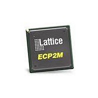
LFE2-20E-5FN484C Lattice, LFE2-20E-5FN484C Datasheet - Page 269

LFE2-20E-5FN484C
Manufacturer Part Number
LFE2-20E-5FN484C
Description
FPGA - Field Programmable Gate Array 21K LUTs 331 I/O DSP 1.2V -5
Manufacturer
Lattice
Series
LatticeECP2r
Datasheet
1.LFE2-12SE-6FN256C.pdf
(389 pages)
Specifications of LFE2-20E-5FN484C
Number Of Macrocells
21000
Number Of Programmable I/os
331
Data Ram Size
282624
Supply Voltage (max)
1.26 V
Maximum Operating Temperature
+ 85 C
Minimum Operating Temperature
0 C
Mounting Style
SMD/SMT
Supply Voltage (min)
1.14 V
Package / Case
FPBGA-484
No. Of Logic Blocks
21000
No. Of Macrocells
10500
No. Of Speed Grades
5
Total Ram Bits
276Kbit
No. Of I/o's
331
Clock Management
DLL, PLL
I/o Supply Voltage
3.465V
Rohs Compliant
Yes
Lead Free Status / RoHS Status
Lead free / RoHS Compliant
Available stocks
Company
Part Number
Manufacturer
Quantity
Price
Company:
Part Number:
LFE2-20E-5FN484C
Manufacturer:
Lattice
Quantity:
135
Company:
Part Number:
LFE2-20E-5FN484C
Manufacturer:
TI
Quantity:
2 658
Company:
Part Number:
LFE2-20E-5FN484C
Manufacturer:
Lattice Semiconductor Corporation
Quantity:
10 000
Part Number:
LFE2-20E-5FN484C
Manufacturer:
LATTICE
Quantity:
20 000
- Current page: 269 of 389
- Download datasheet (5Mb)
Lattice Semiconductor
LFE2M50E/SE Logic Signal Connections: 484 fpBGA (Cont.)
* Supports true LVDS. Other differential signals must be emulated with external resistors.
** These dedicated input pins can be used for GPLLs or GDLLs within the respective quadrant.
***For density migration, board design must take into account that these sysCONFIG pins are dual function for the lower density devices
(ECP2M20 and ECP2M35). They can be either sysCONFIG pins or general purpose I/Os. These pins are dedicated pins for the higher density
devices (ECP2M50, ECP2M70 and ECP2M100).
****Due to packaging bond out option, this DQS does not have all the necessary DQ pins bonded out for a full 8-bit data width.
Note: VCCIO and GND pads are used to determine the average DC current drawn by I/Os between GND/VCCIO connections, or between the
last GND/VCCIO in an I/O bank and the end of an I/O bank. The substrate pads listed in the Pin Table do not necessarily have a one to one
connection with a package ball or pin.
Ball Number
W19
W18
G14
G15
G12
G13
V17
V18
D15
D14
E15
E14
H15
R15
F15
F14
F13
H8
R8
Ball/Pad Function
VCCPLL
VCCPLL
VCCPLL
VCCPLL
NC
NC
NC
NC
NC
NC
NC
NC
NC
NC
NC
NC
NC
NC
NC
LFE2M50E/SE
4-166
Bank
-
-
-
-
-
-
-
-
-
-
-
-
-
-
-
-
-
-
-
LatticeECP2/M Family Data Sheet
Dual Function
Pinout Information
Differential
Related parts for LFE2-20E-5FN484C
Image
Part Number
Description
Manufacturer
Datasheet
Request
R

Part Number:
Description:
IC, LATTICEECP2 FPGA, 420MHZ, QFP-208
Manufacturer:
LATTICE SEMICONDUCTOR
Datasheet:

Part Number:
Description:
FPGA - Field Programmable Gate Array 21K LUTs 331 I/O DSP 1.2V -5
Manufacturer:
Lattice

Part Number:
Description:
FPGA - Field Programmable Gate Array 21K LUTs 402 I/O DSP 1.2V -5
Manufacturer:
Lattice

Part Number:
Description:
FPGA - Field Programmable Gate Array 21K LUTs 193 I/O DSP 1.2V -5 I
Manufacturer:
Lattice

Part Number:
Description:
FPGA - Field Programmable Gate Array 21K LUTs 402 I/O DSP 1.2V -5 I
Manufacturer:
Lattice

Part Number:
Description:
FPGA - Field Programmable Gate Array 21K LUTs 131 I/O DSP 1.2V -5
Manufacturer:
Lattice

Part Number:
Description:
FPGA - Field Programmable Gate Array 21K LUTs 131 I/O DSP 1.2V -5 I
Manufacturer:
Lattice

Part Number:
Description:
IC FPGA 21KLUTS 193I/O 256FPBGA
Manufacturer:
Lattice
Datasheet:
Part Number:
Description:
IC, LATTICEECP2 FPGA, 420MHZ, FPBGA-672
Manufacturer:
LATTICE SEMICONDUCTOR
Datasheet:

Part Number:
Description:
IC, LATTICEECP2 FPGA, 420MHZ, QFP-208
Manufacturer:
LATTICE SEMICONDUCTOR
Datasheet:
Part Number:
Description:
FPGA LatticeECP2 Family 21000 Cells 90nm (CMOS) Technology 1.2V 256-Pin FBGA
Manufacturer:
LATTICE SEMICONDUCTOR
Datasheet:
Part Number:
Description:
FPGA LatticeECP2 Family 21000 Cells 90nm (CMOS) Technology 1.2V 484-Pin FBGA
Manufacturer:
LATTICE SEMICONDUCTOR
Datasheet:
Part Number:
Description:
FPGA LatticeECP2 Family 21000 Cells 90nm (CMOS) Technology 1.2V 484-Pin FBGA
Manufacturer:
LATTICE SEMICONDUCTOR
Datasheet:
Part Number:
Description:
FPGA LatticeECP2 Family 21000 Cells 90nm (CMOS) Technology 1.2V 484-Pin FBGA
Manufacturer:
LATTICE SEMICONDUCTOR
Datasheet:
Part Number:
Description:
FPGA LatticeECP2 Family 21000 Cells 90nm (CMOS) Technology 1.2V 484-Pin FBGA
Manufacturer:
LATTICE SEMICONDUCTOR
Datasheet:


