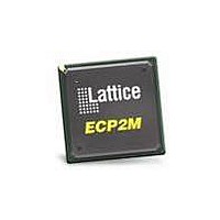
LFE2-20E-5FN484C Lattice, LFE2-20E-5FN484C Datasheet - Page 12

LFE2-20E-5FN484C
Manufacturer Part Number
LFE2-20E-5FN484C
Description
FPGA - Field Programmable Gate Array 21K LUTs 331 I/O DSP 1.2V -5
Manufacturer
Lattice
Series
LatticeECP2r
Datasheet
1.LFE2-12SE-6FN256C.pdf
(389 pages)
Specifications of LFE2-20E-5FN484C
Number Of Macrocells
21000
Number Of Programmable I/os
331
Data Ram Size
282624
Supply Voltage (max)
1.26 V
Maximum Operating Temperature
+ 85 C
Minimum Operating Temperature
0 C
Mounting Style
SMD/SMT
Supply Voltage (min)
1.14 V
Package / Case
FPBGA-484
No. Of Logic Blocks
21000
No. Of Macrocells
10500
No. Of Speed Grades
5
Total Ram Bits
276Kbit
No. Of I/o's
331
Clock Management
DLL, PLL
I/o Supply Voltage
3.465V
Rohs Compliant
Yes
Lead Free Status / RoHS Status
Lead free / RoHS Compliant
Available stocks
Company
Part Number
Manufacturer
Quantity
Price
Company:
Part Number:
LFE2-20E-5FN484C
Manufacturer:
Lattice
Quantity:
135
Company:
Part Number:
LFE2-20E-5FN484C
Manufacturer:
TI
Quantity:
2 658
Company:
Part Number:
LFE2-20E-5FN484C
Manufacturer:
Lattice Semiconductor Corporation
Quantity:
10 000
Part Number:
LFE2-20E-5FN484C
Manufacturer:
LATTICE
Quantity:
20 000
- Current page: 12 of 389
- Download datasheet (5Mb)
Lattice Semiconductor
Table 2-5. DLL Signals
DLLDELA Delay Block
Closely associated with each DLL is a DLLDELA block. This is a delay block consisting of a delay line with taps and
a selection scheme that selects one of the taps. The DCNTL[8:0] bus controls the delay of the CLKO signal. Typi-
cally this is the delay setting that the DLL uses to achieve phase alignment. This results in the delay providing a cal-
ibrated 90° phase shift that is useful in centering a clock in the middle of a data cycle for source synchronous data.
The CLKO signal feeds the edge clock network. Figure 2-7 shows the connections between the DLL block and the
DLLDELA delay block. For more information, please see the list of additional technical documentation at the end of
this data sheet.
Figure 2-7. DLLDELA Delay Block
PLL/DLL Cascading
LatticeECP2/M devices have been designed to allow certain combinations of PLL (GPLL and SPLL) and DLL cas-
cading. The allowable combinations are:
• PLL to PLL supported
• PLL to DLL supported
CLKI
CLKFB
RSTN
ALUHOLD
UDDCNTL
DCNTL[8:0]
CLKOP
CLKOS
LOCK
Signal
GDLLFB_PIO
CLKFB_CK
DLL_PIO
PLL_PIO
Routing
Routing
CLKOP
ECLK1
I/O
O
O
O
O
I
I
I
I
I
Clock input from external pin or routing
Active high freezes the ALU
Synchronous enable signal (hold high for two cycles) from routing
Encoded digital control signals for PIC INDEL and slave delay calibration
The primary clock output
The secondary clock output with fine phase shift and/or division by 2 or by 4
Active high phase lock indicator
DLL feed input from DLL output, clock net, routing or external pin
Active low synchronous reset
* Software selectable
*
*
*
CLKI
CLKFB
CLKI
DCNTL[8:0]
DLLDELA Delay Block
2-9
DLL Block
Description
LatticeECP2/M Family Data Sheet
CLKOP
CLKOS
LOCK
CLKO
Architecture
Related parts for LFE2-20E-5FN484C
Image
Part Number
Description
Manufacturer
Datasheet
Request
R

Part Number:
Description:
IC, LATTICEECP2 FPGA, 420MHZ, QFP-208
Manufacturer:
LATTICE SEMICONDUCTOR
Datasheet:

Part Number:
Description:
FPGA - Field Programmable Gate Array 21K LUTs 331 I/O DSP 1.2V -5
Manufacturer:
Lattice

Part Number:
Description:
FPGA - Field Programmable Gate Array 21K LUTs 402 I/O DSP 1.2V -5
Manufacturer:
Lattice

Part Number:
Description:
FPGA - Field Programmable Gate Array 21K LUTs 193 I/O DSP 1.2V -5 I
Manufacturer:
Lattice

Part Number:
Description:
FPGA - Field Programmable Gate Array 21K LUTs 402 I/O DSP 1.2V -5 I
Manufacturer:
Lattice

Part Number:
Description:
FPGA - Field Programmable Gate Array 21K LUTs 131 I/O DSP 1.2V -5
Manufacturer:
Lattice

Part Number:
Description:
FPGA - Field Programmable Gate Array 21K LUTs 131 I/O DSP 1.2V -5 I
Manufacturer:
Lattice

Part Number:
Description:
IC FPGA 21KLUTS 193I/O 256FPBGA
Manufacturer:
Lattice
Datasheet:
Part Number:
Description:
IC, LATTICEECP2 FPGA, 420MHZ, FPBGA-672
Manufacturer:
LATTICE SEMICONDUCTOR
Datasheet:

Part Number:
Description:
IC, LATTICEECP2 FPGA, 420MHZ, QFP-208
Manufacturer:
LATTICE SEMICONDUCTOR
Datasheet:
Part Number:
Description:
FPGA LatticeECP2 Family 21000 Cells 90nm (CMOS) Technology 1.2V 256-Pin FBGA
Manufacturer:
LATTICE SEMICONDUCTOR
Datasheet:
Part Number:
Description:
FPGA LatticeECP2 Family 21000 Cells 90nm (CMOS) Technology 1.2V 484-Pin FBGA
Manufacturer:
LATTICE SEMICONDUCTOR
Datasheet:
Part Number:
Description:
FPGA LatticeECP2 Family 21000 Cells 90nm (CMOS) Technology 1.2V 484-Pin FBGA
Manufacturer:
LATTICE SEMICONDUCTOR
Datasheet:
Part Number:
Description:
FPGA LatticeECP2 Family 21000 Cells 90nm (CMOS) Technology 1.2V 484-Pin FBGA
Manufacturer:
LATTICE SEMICONDUCTOR
Datasheet:
Part Number:
Description:
FPGA LatticeECP2 Family 21000 Cells 90nm (CMOS) Technology 1.2V 484-Pin FBGA
Manufacturer:
LATTICE SEMICONDUCTOR
Datasheet:


