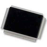
DP83865DVH National Semiconductor, DP83865DVH Datasheet - Page 46

DP83865DVH
Manufacturer Part Number
DP83865DVH
Description
10/100/1000BASE-T TRANSCEIVER, SMD
Manufacturer
National Semiconductor
Specifications of DP83865DVH
Data Rate
1000Mbps
No. Of Ports
1
Ethernet Type
IEEE 802.3u, IEEE 802.3z
Supply Current
430µA
Supply Voltage Range
2.375V To 2.625V, 3.135V To 3.465V
Operating Temperature Range
0°C To +70°C
Interface Type
GMII, MII, RGMII
Rohs Compliant
Yes
Leaded Process Compatible
No
Peak Reflow Compatible (260 C)
No
Lead Free Status / RoHS Status
Lead free / RoHS Compliant
Available stocks
Company
Part Number
Manufacturer
Quantity
Price
Company:
Part Number:
DP83865DVH
Manufacturer:
Texas Instruments
Quantity:
10 000
Company:
Part Number:
DP83865DVH/NOPB
Manufacturer:
NXP
Quantity:
1 000
Company:
Part Number:
DP83865DVH/NOPB
Manufacturer:
Texas Instruments
Quantity:
10 000
www.national.com
3.0 Configuration
3.10.1 MII/GMII Interface
The link speed is determined by Auto-Negotiation, by
strapping options, or by register writes. Based on the
speed linked, an appropriate MAC interface is enabled.
3.10.2 RGMII Interface
The Reduced Gigabit Media Independent Interface
(RGMII) is a proposed standard by HP and 3Com. RGMII
is an alternative data interface to GMII and MII. RGMII
reduces the MAC interface pin count to 12.
The RGMII can be enabled either through strapping option
or MDIO register write. The strapping pins are shared with
CRS/RGMII_SEL0 and TX_CLK/RGMII_SEL1 since CRS
and TX_CLK signals are not used in the RGMII mode.
To enable RGMII through software, Register AUX_CTL
0x12.13:12 should be “10” or “11” binary. Note that
enabling the RGMII interface disables GMII and MII inter-
faces.
3.11 Clock to MAC Enable
The DP83865 has a clock output (pin 85) that can be used
as a reference clock for other devices such as MAC or
switch silicon. The Clock to MAC output can be enabled
through strapping pins.
The Clock to MAC Enable Strap (pin 88) enables the clock
output. The output frequency can be selected between 25
MHz or 125 MHz. The frequency selection strapping pin is
combined with COL (pin 39), CLK_MAC_FRQ.
CRS/RGMII_SEL0
TX_CLK/RGMII_SEL1
CRS/RGMII_SEL0
TX_CLK/RGMII_SEL1
SPEED[1:0] Link Strapped
00
01
10
11
Link Negotiated
Table 45. RGMII Strapping for 3COM mode
100BASE-TX
1000BASE-T
Table 44. RGMII Strapping for HP mode
10BASE-T
Table 42. Auto-Negotiation Disabled
Table 43. Auto-Negotiation Enabled
Signal
Signal
100BASE-TX
1000BASE-T
10BASE-T
reserved
(Continued)
Controller I/F
GMII/RGMII
Controller I/F
Pin
Pin
40
60
40
60
GMII/RGMII
MII
MII
MII
MII
---
Strap
Strap
0
1
1
1
46
Note that upon power up, the clock output is available after
GPHY goes through its internal reset and initialization pro-
cess. The clock output can be interrupted when GPHY is
going through software reset.
3.12 MII/GMII/RGMII Isolate Mode
The DP83865 can be placed into MII/GMII/RGMII Isolate
mode by writing to bit 10 of the BMCR 0x00.
3.12.1 10/100 Mbps Isolate Mode
In Isolation Mode, the DP83865 does not respond to
packet data present at TXD[3:0], TX_EN, and TX_ER
inputs and presents a high impedance on the TX_CLK,
RX_CLK, RX_DV, RX_ER, RXD[3:0], COL, and CRS out-
puts. The DP83865 will continue to respond to all manage-
ment transactions through MDIO.
While in Isolate mode, all medium access operations are
disabled.
3.12.2 1000 Mbps Isolate Mode
During 1000 Mbps operation, the isolate mode will TRI-
STATE the GMII outputs of the GigPHYTER V. The PHY
also enters into the power down mode. All medium access
operations are halted. The only way to communicate to the
PHY is through MDIO management port.
3.13 Loopback Mode
The DP83865 includes a Loopback Test mode for easy
board diagnostics. The Loopback mode is selected through
bit 14 (Loopback) of BMCR 0x00. Writing 1 to this bit
enables MII/GMII transmit data to be routed to the MII/GMII
receive outputs. While in Loopback mode the data will not
be transmitted onto the media. This is true for 10Mbps, 100
Mbps, as well 1000 Mbps data.
In 10BASE-T, 100BASE-TX, 1000BASE-T Loopback mode
the data is routed through the PCS and PMA layers into the
PMD sublayer before it is looped back. Therefore, in addi-
tion to serving as a board diagnostic, this mode serves as
quick functional verification of the device.
3.14 IEEE 802.3ab Test Modes
IEEE 802.3ab specification for 1000BASE-T requires that
the PHY layer be able to generate certain well defined test
patterns on TX outputs. Clause 40 section 40.6.1.1.2 “Test
Modes” describes these tests in detail. There are four test
modes as well as the normal operation mode. These
modes can be selected by writing to the 1KTCR 0x09 as
shown.
bit 15
1
0
0
0
0
bit 14
Table 46. IEEE Test Mode Select
0
1
1
0
0
bit 13
0
1
0
1
0
Test Mode Selected
= Normal Operation
= Test Mode 4
= Test Mode 3
= Test Mode 2
= Test Mode 1


