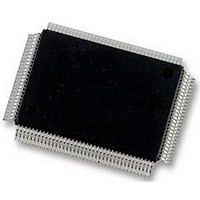
DP83865DVH National Semiconductor, DP83865DVH Datasheet - Page 63

DP83865DVH
Manufacturer Part Number
DP83865DVH
Description
10/100/1000BASE-T TRANSCEIVER, SMD
Manufacturer
National Semiconductor
Specifications of DP83865DVH
Data Rate
1000Mbps
No. Of Ports
1
Ethernet Type
IEEE 802.3u, IEEE 802.3z
Supply Current
430µA
Supply Voltage Range
2.375V To 2.625V, 3.135V To 3.465V
Operating Temperature Range
0°C To +70°C
Interface Type
GMII, MII, RGMII
Rohs Compliant
Yes
Leaded Process Compatible
No
Peak Reflow Compatible (260 C)
No
Lead Free Status / RoHS Status
Lead free / RoHS Compliant
Available stocks
Company
Part Number
Manufacturer
Quantity
Price
Company:
Part Number:
DP83865DVH
Manufacturer:
Texas Instruments
Quantity:
10 000
Company:
Part Number:
DP83865DVH/NOPB
Manufacturer:
NXP
Quantity:
1 000
Company:
Part Number:
DP83865DVH/NOPB
Manufacturer:
Texas Instruments
Quantity:
10 000
5.0 Design Guide
The design guide in conjunction with the Reference Design
Schematics/BOM is intended to provide information to
assist in the design and layout of the DP83865 Gigabit
Ethernet Transceiver. The design guide covers the follow-
ing topics:
— Hardware Reset
— Clocks
— Power Supply Decoupling
— Sensitive Supply Pins
— PCB Layer Stacking
— Layout Notes on MAC Interface
— Twisted Pair Interface
— RJ-45 Connections
— Unused Pins / Reserved Pins
— LED/Strapping Configuration
— I/O Voltage Considerations
— Power-up Recommendations
— Compoment Selection
There are a number of ways to terminate clock traces when
an oscillator is used. The commonly used types are series
and parallel termination. Series termination consumes less
power and it is the recommended termination. The value of
the series termination resistor is chosen to match the trace
characteristics impedance. For example, if the clock
source has an output impedance of 20
trace has the characteristic impedance Zo = 50 then Rs =
50 - 20 = 30 . The series source termination Rs should be
placed close to the output of the oscillator.
The parallel termination consumes more power than series
termination, and yields faster rise and fall times. The value
of the termination is equal to the trace characteristic imped-
ance, R
placed close to the CLOCK_IN pin to eliminate reflections.
In cases there are multiple PHY deivces reside on the
same board, it may be cost effective to use one oscillator
with a high speed PLL clock distribution driver. Connecting
multiple clock inputs in a daisy chained style should be
avoided, especially when series termination is applied.
No termination is necessary if a crystal is used. The crystal
should be placed as close as possible to the CLOCK pins.
The capacitors C1 and C2 are used to adjust the load
capacitance on these pins. (Figure 13.) The total load
capacitance (C1, C2 and crystal) must be within a certain
range for the DP83865 to function properly (see Table 55
for crystal requirements). The parallel resistor R
C
C
25MHz
2
1
T
Crystal option circuit
= Zo.
CLOCK_OUT
The parallel termination R
CLOCK_IN
R
T
DP83865
and the clock
Figure 13. Clock Input Circuit
T
T
should be
is recom-
V
DD
= 3.3 V
GND
V
DD
63
25MHz
5.1 Hardware Reset
The active low RESET pin 33 should be held low for a min-
imum of 150 s to allow hardware reset. For timing details
see Section 6.2. There is no on-chip internal power-on
reset and the DP83865 requires an external reset signal
applied to the RESET pin.
5.2 Clocks
The CLOCK_IN pin is the 25 MHz clock input to the
DP83865 used by the internal PLL. This input should come
from a 25 MHz clock oscillator or a crystal. (Check
Section 5.13.1 for component requirements.) When using
a crystal, CLOCK_OUT must be connected to the second
terminal of the crystal. For usage with a oscillator the
CLOCK_OUT pin should be left floating.
The output of the clock signal requires termination consid-
eration. The termination requirement depends on the trace
length of the clock signal. No series or load termination is
required for short traces less than 3 inches. For longer
traces termination resistors are recommended.
mended by some crystal vendors. Refer to the vendor’s
crystal datasheet for details.
Adequate and proper decoupling is important to the clock
oscillator performance. A multilayer ceramic chip capacitor
should be placed as close to the oscillator’s VDD pin as
possible to supply the additional current during the tran-
sient switching.
EMI is another consideration when designing the clock cir-
cuitry. The EMI field strength is proportional to the current
flow, frequency, and loop area. By applying series termina-
tion, the current flow is less than parallel termination and
the edge speed is slower, making it desirable for EMI con-
siderations. The loop area is defined as the trace length
times the distance to the ground plane, i.e., the current
return path. Keeping the clock trace as short as possible
reduces the loop area that reduces EMI.
It is best to place the oscillator towards the center of the
PCB rather than at the edge. The radiated magnetic field
tends to be stronger when traces are running along the
PCB edge. If the trace has to run along the edge of the
board, make sure the trace to board edge distance is larger
than the trace to ground plane distance. This makes the
field around the trace more easily coupled to the ground
than radiating off the edge. If the clock trace is placed on
the surface layer, placing a parallel ground trace on each
side of the clock trace localizes the EMI and also prevent
crosstalk to adjacent traces. Burying the clock trace in
EN
Oscillator option circuit
(Optional)
Zo
R
T
CLOCK_OUT
CLOCK_IN
DP83865
www.national.com


