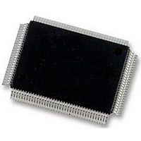
DP83865DVH National Semiconductor, DP83865DVH Datasheet - Page 52

DP83865DVH
Manufacturer Part Number
DP83865DVH
Description
10/100/1000BASE-T TRANSCEIVER, SMD
Manufacturer
National Semiconductor
Specifications of DP83865DVH
Data Rate
1000Mbps
No. Of Ports
1
Ethernet Type
IEEE 802.3u, IEEE 802.3z
Supply Current
430µA
Supply Voltage Range
2.375V To 2.625V, 3.135V To 3.465V
Operating Temperature Range
0°C To +70°C
Interface Type
GMII, MII, RGMII
Rohs Compliant
Yes
Leaded Process Compatible
No
Peak Reflow Compatible (260 C)
No
Lead Free Status / RoHS Status
Lead free / RoHS Compliant
Available stocks
Company
Part Number
Manufacturer
Quantity
Price
Company:
Part Number:
DP83865DVH
Manufacturer:
Texas Instruments
Quantity:
10 000
Company:
Part Number:
DP83865DVH/NOPB
Manufacturer:
NXP
Quantity:
1 000
Company:
Part Number:
DP83865DVH/NOPB
Manufacturer:
Texas Instruments
Quantity:
10 000
www.national.com
4.0 Functional Description
1000BASE-T transceiver and shows the functionality of the
PCS receiver.
The major sub functional blocks of the PCS Receiver
include:
— Delay Skew Compensation
— Delay Skew Control
— Forward Error Correction (FEC)
— Descrambler Subsystem
— Receive State Machine
— ADC/DAC/Timing Subsystem
The requirements for the PCS receive functionality are
defined in the IEEE 802.3ab specification in section
40.3.1.4 “PCS Receive function”.
4.4.1 Delay Skew Compensation
This is a mechanism used to align the received data from
the four PMA receivers and to determine the correct spa-
cial ordering of the four incoming twisted pairs, i.e., which
twisted pair carries A
skewed and ordered symbols are then presented to the
Forward Error Correction (FEC) Decoder. The differential
time or time delay skew is due to the differences in length
of each of the four pairs of twisted wire in the CAT-5 cable,
manufacturing variation of the insulation of the wire pairs,
and in some cases, differences in insulation materials used
in the wire pairs. Correct symbol order to the FEC is
required, since the receiver does not have prior knowledge
of the order of the incoming twisted pairs within the CAT-5
cable.
4.4.2 Delay Skew Control
This sub block controls the delay skew compensation func-
tion by providing the necessary controls to allow for com-
pensation in two dimensions. The two dimensions are
referring to time and position. The time factor is the delay
skew between the four incoming data streams from the
PMA RX A, B, C, and D. This delay skew originates back at
the input to the ADC/DAC/TIMING subsystem. Since the
receiver initially does not know the ordering of the twisted
pairs, correct ordering must be determined automatically
by the receiver during start-up. Delay skew compensation
and twisted pair ordering is part of the training function per-
formed during start-up mode of operation.
4.4.3 Forward Error Correction (FEC) Decoder
The FEC Decoder decodes the quartet of quinary (PAM-5)
symbols and generates the corresponding Sd
words. The FEC decoder uses a standard 8 state Trellis
code operation. Initially, Sd
bit ordering, however, correct ordering is established by the
reordering algorithm at start-up.
4.4.4 Descrambler Subsystem
The descrambler block performs the reverse scrambling
function that was implemented in the transmit section. This
sub block works in conjunction with the delay skew control.
It provides the receiver generated Sd
ison in the delay skew control function.
n
, which one carries B
n
[3:0] may not have the proper
n
[3:0] bits for compar-
(Continued)
n
, etc. The de-
n
binary
52
4.4.5 Receive State Machine
The state machine operation is defined in IEEE 802.3ab
section 40.3.1.4. In summary, it provides the necessary
receive control signals of RX_DV and RX_ER to the GMII.
In specific conditions defined in the IEEE 802.3ab specifi-
cation, it generates RXD[7:0] data.
4.4.6 ADC/DAC/Timing Subsystem
The 1000BASE-T receive section consists of 4 channels,
each receiving IEEE 802.3ab compliant PAM-5 coded data
including Partial Response (PR) shaping at 125 MBaud
over a maximum of a 100 m of CAT-5 cable. The 4 pairs of
receive input pins are AC coupled through the magnetics to
the CAT-5 cable. Each receive pin pair is differentially ter-
minated into an external 100W resistor to match the cable
impedance. Each receive channel consists of a high preci-
sion Analog to Digital data converter (ADC) which quan-
tizes the incoming data into a digital word at the rate of 125
Mb/s. The ADC is sampled with a clock of 125 MHz which
has been recovered from the incoming data stream.
The 1000BASE-T transmit section consists of 4 channels,
each transmitting IEEE 802.3ab compliant 17-level PAM-5
data at 125 M symbols/second. The 4 pairs of transmit out-
put pins are AC coupled through the magnetics to the CAT-
5 cable. Each transmit pin pair is differentially terminated
into an external 100W resistor to match the cable imped-
ance. Each transmit channel consists of a Digital to Analog
data converter (DAC) and line driver capable of producing
17 discrete levels corresponding to the PR shaping of a
PAM-5 coded data stream. Each DAC is clocked with the
internal 125 MHz clock in the MASTER mode, and the
recovered receive clock in the SLAVE mode operation.
The DP83865 incorporates a sophisticated Clock Genera-
tion Module (CGM) which supports 10/100/1000 modes of
operation with an external 25 MHz clock reference (±50
ppm). The Clock Generation module internally generates
multiple phases of clocks at various frequencies to support
high precision and low jitter Clock Recovery Modules
(CRM) for robust data recovery, and to support accurate
low jitter transmission of data symbols in the MASTER and
SLAVE mode operations.
4.5 Gigabit MII (GMII)
The Gigabit Media Independent Interface (GMII) is
intended for use between Ethernet PHYs and Station Man-
agement (STA) entities and is selected by either hardware
or software configuration. The purpose of GMII is to make
various physical media transparent to the MAC layer.
The GMII Interface accepts either GMII or MII data, control
and status signals and routes them either to the
1000BASE-T, 100BASE-TX, or 10BASE-T modules,
respectively.


