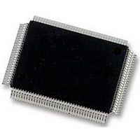
DP83865DVH National Semiconductor, DP83865DVH Datasheet - Page 68

DP83865DVH
Manufacturer Part Number
DP83865DVH
Description
10/100/1000BASE-T TRANSCEIVER, SMD
Manufacturer
National Semiconductor
Specifications of DP83865DVH
Data Rate
1000Mbps
No. Of Ports
1
Ethernet Type
IEEE 802.3u, IEEE 802.3z
Supply Current
430µA
Supply Voltage Range
2.375V To 2.625V, 3.135V To 3.465V
Operating Temperature Range
0°C To +70°C
Interface Type
GMII, MII, RGMII
Rohs Compliant
Yes
Leaded Process Compatible
No
Peak Reflow Compatible (260 C)
No
Lead Free Status / RoHS Status
Lead free / RoHS Compliant
Available stocks
Company
Part Number
Manufacturer
Quantity
Price
Company:
Part Number:
DP83865DVH
Manufacturer:
Texas Instruments
Quantity:
10 000
Company:
Part Number:
DP83865DVH/NOPB
Manufacturer:
NXP
Quantity:
1 000
Company:
Part Number:
DP83865DVH/NOPB
Manufacturer:
Texas Instruments
Quantity:
10 000
www.national.com
5.0 Design Guide
board space, the adjacent unused input pins can be
grouped and tied together with a single resistor.
The number of unused pins and which pins become
unused pins highly depend on the individual application the
DP83865 is used in. Refer to Section 1.0 for each individ-
ual pin that is not used.
Reserved pins must be left floating.
5.11 I/O Voltage Considerations
The VDD_SEL_STRAP pin selects which I/O voltage
(IO_VDD) is used in an application. The choice is between
2.5V and 3.3V. If the designer was to choose 2.5V an addi-
tional 3.3V supply could be saved. However, the deciscion
should not be soley based on saving components but
rather on the environment the DP83865 operates in.
IO_VDD supplies the pins for “MAC Interfaces”, “Manage-
ment Interface”, “JTAG Interface”, “Device Configuration
and LED Interface” and “Reset”. All input pins are either
2.5V or 3.3V compatible. All output pins will have a high
level equal to IO_VDD. The designer must make sure that
all connected devices are compatible with the logic ‘1’ state
of the DP83865 (that is either 2.5V or 3.3V).
If 2.5V IOVDD is selected, do not over drive the GPHY
input with 3.3V logic. The over driving may cause exces-
sive EMI noise and reduce GPHY performance. Over driv-
ing may also cause higher power consumption.
5.12 Power-up Recommendations
During power-up, the power supply voltages are not avail-
able immediately but ramp up relatively slow compared to
the clock period of the system clock (CLOCK_IN). How
quickly a supply voltage reaches the “power good” level of
Frequency Tolerance
Frequency Tolerance
Frequency Stability
Frequency Stability
Load Capacitance
Jitter (short term)
Jitter (long term)
Rise/Fall Time
Parameter
Parameter
Frequency
Frequency
Symmetry
Logic 0
Logic 1
(Continued)
Min
Min
40
90
15
-
-
-
-
-
-
-
-
-
-
Table 54. 25 MHz Oscillator Requirements
Table 55. 25 MHz Crystal Requirements
Typ
Typ
25
25
-
-
-
-
-
-
-
-
-
-
-
Max
Max
200
25
60
10
40
6
-
50
50
-
-
50
50
68
typically 95% of its nominal voltage varies from design to
design.
There is no specific requirement for power-up sequence for
the DP83865. However, if it is desirable to control the
power up order, it is theoretically advised to power up
CORE_VDD supply first. If there is no such ability all sup-
plies can be powered up at the same time. There is no
known sequence to date that can cause DP83865 in a
latch-up or lock up condition.
In any event, the RESET signal should be held low until
after all power supplies have reached their nominal volt-
ages. See Section 6.2 for additional requirements.
5.13 Component Selection
5.13.1 Oscillator
The requirements of 25 Mhz oscillators and crystals are
listed in Table 54 and Table 55. Some recommended man-
ufacuturers are listed in Table 56.
In the cases where multiple clock sources with the same
frequency are needed, it is recommended to use a clock
distribution circuit in conjuction with a single freqeuncy
generator. These devices may be obtained from vendors
such as Texas Instrument, Pericom, and Integrated Device
Technology.
Note that the jitter specification was derived from maximum
capacitance load, worst case supply voltage, and wide
temperature range. The actual allowable jitter number may
be significantly higer when driving the DP83865 clock input
under normal operating conditions. Please consult the
respective vendors for specifics.
Units
Units
MHz
ppm
ppm
MHz
ppm
ppm
pF
ns
ps
ps
%
%
%
and C2 (see Section 5.2 for dimension-
Total load capacitance including C1
Cycle-to-cycle, driving 10 pF load
IO_VDD = 2.5 or 3.3V nominal
IO_VDD = 2.5 or 3.3V nominal
Accumulative over 10 s
0 °C to 70 °C
0 °C to 70 °C
1 year aging
1 year aging
Condition
Condition
20 - 80 %
ing)
-
-
-


