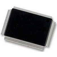
DP83865DVH National Semiconductor, DP83865DVH Datasheet - Page 49

DP83865DVH
Manufacturer Part Number
DP83865DVH
Description
10/100/1000BASE-T TRANSCEIVER, SMD
Manufacturer
National Semiconductor
Specifications of DP83865DVH
Data Rate
1000Mbps
No. Of Ports
1
Ethernet Type
IEEE 802.3u, IEEE 802.3z
Supply Current
430µA
Supply Voltage Range
2.375V To 2.625V, 3.135V To 3.465V
Operating Temperature Range
0°C To +70°C
Interface Type
GMII, MII, RGMII
Rohs Compliant
Yes
Leaded Process Compatible
No
Peak Reflow Compatible (260 C)
No
Lead Free Status / RoHS Status
Lead free / RoHS Compliant
Available stocks
Company
Part Number
Manufacturer
Quantity
Price
Company:
Part Number:
DP83865DVH
Manufacturer:
Texas Instruments
Quantity:
10 000
Company:
Part Number:
DP83865DVH/NOPB
Manufacturer:
NXP
Quantity:
1 000
Company:
Part Number:
DP83865DVH/NOPB
Manufacturer:
Texas Instruments
Quantity:
10 000
4.0 Functional Description
The DP83865 is a full featured 10/100/1000 Ethernet Phys-
ical layer (PHY) chip. It consists of a digital 10/100/1000
Mb/s core with a common TP interface. It also has a com-
bined versitle MAC interface that is capable of interfacing
with MII and GMII controller interfaces. In this section, the
following topics are covered:
— 1000BASE-T PCS Transmitter
— 1000BASE-T PMA Transmitter
— 1000BASE-T PMA Receiver
— 1000BASE-T PCS Receiver
— Gigabit MII (GMII)
— Reduced GMII (RGMII)
— 10BASE-T and 100BASE-TX Transmitter
— 10BASE-T and 100BASE-TX Receiver
— Media Dependent Interface (MII)
The 1000BASE-T transceiver includes PCS (Physical Cod-
ing Sublayer) Transmitter, PMA (Physical Medium Attach-
ment) Transmitter, PMA Receiver and PCS Receiver. The
1000BASE-T functional block diagram is shown in section
“ Block Diagram” on page 2.
4.1 1000BASE-T PCS Transmitter
The PCS transmitter comprises several functional blocks
that convert the 8-bit TXD
symbols passed onto the PMA function. The block diagram
of the PCS transmitter data path in Figure 2 provides an
overview of each of the architecture within the PCS trans-
mitter.
The PCS transmitter consists of eight sub blocks:
— LFSR (Linear Feedback Shift Register)
— Data scrambler and symbol sign scrambler word gener-
— Scrambler bit generator
— Data scrambler
— Convolutional encoder
— Bit-to-symbol quinary symbol mapping
— Sign scrambler nibble generator
— Symbol sign scrambler
The requirements for the PCS transmit functionality are
also defined in the IEEE 802.3ab specification section
40.3.1.3 “PCS Transmit function”.
4.1.1 Linear Feedback Shift Register (LFSR)
The side-stream scrambler function uses a LFSR imple-
menting one of two equations based on the mode of opera-
tion, i.e., a master or a slave. For master operation, the
equation is
g
For slave operation, the equation is
g
The 33-bit data output, Scr
to the data scrambler and symbol sign scrambler word gen-
erator.
M
S
(x) = 1 + x
(x) = 1 + x
ator
20
13
+ x
+ x
33
33
n
n
[32:0], of this block is then fed
data from the GMII to PAM-5
49
4.1.2 Data and Symbol Sign Scrambler Word Generator
The word generator uses the Scr
scrambled values. The following signals are generated:
Sx
The 4-bit Sx
scrambler bit generator. The 4-bit Sg
provided to the sign scrambler nibble generator.
4.1.3 Scrambler Bit Generator
This sub block uses the Sx
tx_mode and tx_enable signals to generate the Sc
that is further scrambled based on the condition of the
tx_mode and tx_enable signal. The tx_mode signal indi-
cates sending idles (SEND_I), sending zeros (SEND_Z) or
sending idles/data (SEND_N). The tx_mode signal is gen-
erated by the micro controller function. The tx_enable sig-
nal is either asserted to indicate data transmission is
occurring or deasserted when there is no data transmis-
sion. The PCS Data Transmission Enable state machine
generates the tx_enable signal.
The 8-bit Sc
scrambler functional block.
4.1.4 Data Scrambler
The Data Scrambler generates scrambled data by accept-
ing the TxD
based on various inputs.
The data scrambler generates the 8-bit Sd
which scrambles the TxD
values and the accompanying control signals.
All 8-bits of Sd
symbol mapping block, while 2-bits, Sd
the convolutional encoder.
4.1.5 Convolutional Encoder
The encoder uses Sd
an additional data bit, which is called Sd
The one clock delayed versions cs
the data scrambler block. This Sd
the bit-to-symbol quinary symbol mapping function.
4.1.6 Bit-to-Symbol Quinary Symbol Mapping
This block implements the IEEE 802.3ab specification
Tables 40-1 and 40-2 Bit-to-Symbol Mapping for even and
odd subsets. It takes the 9-bit Sd
to the appropriate quinary symbols as defined by the
tables.
The output of this block generates the TA
TD
4.1.7 Sign Scrambler Nibble Generator
Sign Scrambler Nibble Generator performs some further
scrambling of the sign values Sg
by the data and symbol sign scrambler word generator.
The sign scrambling is dependent on the tx_enable signal.
The S
onto the symbol sign scrambler function.
n
n
[3:0], Sy
symbols that passed onto the symbol sign scrambler.
n
A
n
, S
n
n
n
n
n
[3:0], and Sg
[3:0] and Sy
[7:0] data from the GMII and scrambling it
B
[7:0] signals are then passed onto the data
n
, S
n
[7:0] are passed onto the bit-to-quinary
n
C
n
n
, and S
[7:6] bits and tx_enable to generate
n
n
n
[3:0] values are then sent to the
[3:0].
n
data based primarily on the Sc
and Sy
n
D
n
n
n
n
[32:0] to generate further
[8:0] data and converts it
n
outputs are then passed
[3:0] that are generated
[8] bit is then passed to
n
n-1
signals along with the
n
[3:0] sign values are
[1:0] are passed to
n
n
[8].
[7:6], are fed into
n
, TB
www.national.com
n
[7:0] value,
n
, TC
n
n
, and
[7:0],
n


