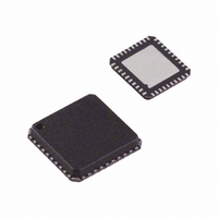
ADUC7020BCPZ62I-RL Analog Devices Inc, ADUC7020BCPZ62I-RL Datasheet - Page 19

ADUC7020BCPZ62I-RL
Manufacturer Part Number
ADUC7020BCPZ62I-RL
Description
IC,MICROCONTROLLER,16-BIT,ARM7 CPU,CMOS,LLCC,40PIN,PLASTIC
Manufacturer
Analog Devices Inc
Series
MicroConverter® ADuC7xxxr
Datasheet
1.USB-I2CLIN-CONV-Z.pdf
(96 pages)
Specifications of ADUC7020BCPZ62I-RL
Core Processor
ARM7
Core Size
16/32-Bit
Speed
44MHz
Connectivity
EBI/EMI, I²C, SPI, UART/USART
Peripherals
PLA, PWM, PSM, Temp Sensor, WDT
Number Of I /o
14
Program Memory Size
62KB (62K x 8)
Program Memory Type
FLASH
Ram Size
8K x 8
Voltage - Supply (vcc/vdd)
2.7 V ~ 3.6 V
Data Converters
A/D 5x12b; D/A 4x12b
Oscillator Type
Internal
Operating Temperature
-40°C ~ 125°C
Package / Case
40-LFCSP
Lead Free Status / RoHS Status
Lead free / RoHS Compliant
For Use With
EVAL-ADUC7020QSZ - KIT DEV ADUC7020 QUICK STARTEVAL-ADUC7020MKZ - KIT MINI DEV FOR ADUC7026/7027
Eeprom Size
-
Lead Free Status / RoHS Status
Lead free / RoHS Compliant
Available stocks
Company
Part Number
Manufacturer
Quantity
Price
Part Number:
ADUC7020BCPZ62I-RL
Manufacturer:
ADI/亚德诺
Quantity:
20 000
7019/7020
10
11
12
13
14
15
16
17
18
19
20
21
22
23
24
25
26
27
28
29
30
31
32
33
34
Pin No.
7021
10
11
12
13
14
15
16
17
18
19
20
21
22
23
24
25
26
27
28
29
30
31
32
33
‒
7022
9
10
11
12
13
14
15
16
17
18
19
20
21
22
23
24
25
26
27
28
29
30
31
32
‒
Mnemonic
BM/P0.0/CMP
P0.6/T1/MRST/PLAO[3]
TCK
TDO
IOGND
IOV
LV
DGND
P0.3/TRST/ADC
RST
IRQ0/P0.4/PWM
IRQ1/P0.5/ADC
P2.0/SPM9/PLAO[5]/CONV
P0.7/ECLK/XCLK/SPM8/PLAO[4]
XCLKO
XCLKI
P1.7/SPM7/PLAO[0]
P1.6/SPM6/PLAI[6]
P1.5/SPM5/PLAI[5]/IRQ3
P1.4/SPM4/PLAI[4]/IRQ2
P1.3/SPM3/PLAI[3]
P1.2/SPM2/PLAI[2]
P1.1/SPM1/PLAI[1]
P1.0/T1/SPM0/PLAI[0]
P4.2/PLAO[10]
DD
DD
OUT
BUSY
BUSY
TRIP
/PLAI[7]
/PLAO[2]
/PLAO[1]
START
Rev. C | Page 19 of 96
Description
Multifunction I/O Pin. Boot Mode (BM). The ADuC7019/20/21/22 enter
serial download mode if BM is low at reset and execute code if BM is
pulled high at reset through a 1 kΩ resistor/General-Purpose Input and
Output Port 0.0/Voltage Comparator Output/Programmable Logic Array
Input Element 7.
Multifunction Pin. Driven low after reset. General-Purpose Output Port 0.6/
Timer1 Input/Power-On Reset Output/Programmable Logic Array Output
Element 3.
Test Clock, JTAG Test Port Input. Debug and download access. This pin has
an internal pull-up resistor to IOV
resistor (~100K) is also required to ensure that the part does not enter an
erroneous state.
Test Data Out, JTAG Test Port Output. Debug and download access.
Ground for GPIO (see Table 78). Typically connected to DGND.
3.3 V Supply for GPIO (see Table 78) and Input of the On-Chip Voltage
Regulator.
2.6 V Output of the On-Chip Voltage Regulator. This output must be
connected to a 0.47 μF capacitor to DGND only.
Ground for Core Logic.
General-Purpose Input and Output Port 0.3/Test Reset, JTAG Test Port Input/
ADC
Reset Input, Active Low.
Multifunction I/O Pin. External Interrupt Request 0, Active High/General-
Purpose Input and Output Port 0.4/PWM Trip External Input/Programmable
Logic Array Output Element 1.
Multifunction I/O Pin. External Interrupt Request 1, Active High/General-
Purpose Input and Output Port 0.5/ADC
Logic Array Output Element 2.
Serial Port Multiplexed. General-Purpose Input and Output Port 2.0/UART/
Programmable Logic Array Output Element 5/Start Conversion Input Signal
for ADC.
Serial Port Multiplexed. General-Purpose Input and Output Port 0.7/
Output for External Clock Signal/Input to the Internal Clock Generator
Circuits/UART/ Programmable Logic Array Output Element 4.
Output from the Crystal Oscillator Inverter.
Input to the Crystal Oscillator Inverter and Input to the Internal Clock
Generator Circuits.
Serial Port Multiplexed. General-Purpose Input and Output Port 1.7/UART,
SPI/Programmable Logic Array Output Element 0.
Serial Port Multiplexed. General-Purpose Input and Output Port 1.6/UART,
SPI/Programmable Logic Array Input Element 6.
Serial Port Multiplexed. General-Purpose Input and Output Port 1.5/UART,
SPI/Programmable Logic Array Input Element 5/External Interrupt
Request 3, Active High.
Serial Port Multiplexed. General-Purpose Input and Output Port 1.4/UART,
SPI/Programmable Logic Array Input Element 4/External Interrupt
Request 2, Active High.
Serial Port Multiplexed. General-Purpose Input and Output Port 1.3/UART,
I2C1/Programmable Logic Array Input Element 3.
Serial Port Multiplexed. General-Purpose Input and Output Port 1.2/UART,
I2C1/Programmable Logic Array Input Element 2.
Serial Port Multiplexed. General-Purpose Input and Output Port 1.1/UART,
I2C0/Programmable Logic Array Input Element 1.
Serial Port Multiplexed. General-Purpose Input and Output Port 1.0/
Timer1 Input/UART, I2C0/Programmable Logic Array Input Element 0.
General-Purpose Input and Output Port 4.2/Programmable Logic Array
Output Element 10.
BUSY
Signal Output.
ADuC7019/20/21/22/24/25/26/27/28/29
DD
. In some cases an external pull-up
BUSY
Signal Output/Programmable


