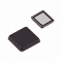
ADUC7020BCPZ62I-RL Analog Devices Inc, ADUC7020BCPZ62I-RL Datasheet - Page 65

ADUC7020BCPZ62I-RL
Manufacturer Part Number
ADUC7020BCPZ62I-RL
Description
IC,MICROCONTROLLER,16-BIT,ARM7 CPU,CMOS,LLCC,40PIN,PLASTIC
Manufacturer
Analog Devices Inc
Series
MicroConverter® ADuC7xxxr
Datasheet
1.USB-I2CLIN-CONV-Z.pdf
(96 pages)
Specifications of ADUC7020BCPZ62I-RL
Core Processor
ARM7
Core Size
16/32-Bit
Speed
44MHz
Connectivity
EBI/EMI, I²C, SPI, UART/USART
Peripherals
PLA, PWM, PSM, Temp Sensor, WDT
Number Of I /o
14
Program Memory Size
62KB (62K x 8)
Program Memory Type
FLASH
Ram Size
8K x 8
Voltage - Supply (vcc/vdd)
2.7 V ~ 3.6 V
Data Converters
A/D 5x12b; D/A 4x12b
Oscillator Type
Internal
Operating Temperature
-40°C ~ 125°C
Package / Case
40-LFCSP
Lead Free Status / RoHS Status
Lead free / RoHS Compliant
For Use With
EVAL-ADUC7020QSZ - KIT DEV ADUC7020 QUICK STARTEVAL-ADUC7020MKZ - KIT MINI DEV FOR ADUC7026/7027
Eeprom Size
-
Lead Free Status / RoHS Status
Lead free / RoHS Compliant
Available stocks
Company
Part Number
Manufacturer
Quantity
Price
Part Number:
ADUC7020BCPZ62I-RL
Manufacturer:
ADI/亚德诺
Quantity:
20 000
Table 83. GPxDAT Registers
Name
GP0DAT
GP1DAT
GP2DAT
GP3DAT
GP4DAT
1
GPxDAT are Port x configuration and data registers. They
configure the direction of the GPIO pins of Port x, set the
output value for the pins configured as output, and store the
input value of the pins configured as input.
Table 84. GPxDAT MMR Bit Descriptions
Bit
31:24
23:16
15:8
7:0
Table 85. GPxSET Registers
Name
GP0SET
GP1SET
GP2SET
GP3SET
GP4SET
1
GPxSET are data set Port x registers.
Table 86. GPxSET MMR Bit Descriptions
Bit
31:24
23:16
15:0
Table 87. GPxCLR Registers
Name
GP0CLR
GP1CLR
GP2CLR
GP3CLR
GP4CLR
1
GPxCLR are data clear Port x registers.
X = 0, 1, 2, or 3.
X = 0, 1, 2, or 3.
X = 0, 1, 2, or 3.
Description
Direction of the data. Set to 1 by user to configure
the GPIO pin as an output. Cleared to 0 by user to
configure the GPIO pin as an input.
Port x data output.
Reflect the state of Port x pins at reset (read only).
Port x data input (read only).
Description
Reserved.
Data Port x set bit. Set to 1 by user to set bit on Port x;
also sets the corresponding bit in the GPxDAT MMR.
Cleared to 0 by user; does not affect the data out.
Reserved.
Address
0xFFFFF420
0xFFFFF430
0xFFFFF440
0xFFFFF450
0xFFFFF460
Address
0xFFFFF424
0xFFFFF434
0xFFFFF444
0xFFFFF454
0xFFFFF464
Address
0xFFFFF428
0xFFFFF438
0xFFFFF448
0xFFFFF458
0xFFFFF468
Default Value
0x000000XX
0x000000XX
0x000000XX
0x000000XX
0x000000XX
Default Value
0x000000XX
0x000000XX
0x000000XX
0x000000XX
0x000000XX
Default Value
0x000000XX
0x000000XX
0x000000XX
0x000000XX
0x000000XX
1
1
1
Access
R/W
R/W
R/W
R/W
R/W
Access
W
W
W
W
W
Access
W
W
W
W
W
Rev. C | Page 65 of 96
Table 88. GPxCLR MMR Bit Descriptions
Bit
31:24
23:16
15:0
SERIAL PORT MUX
The serial port mux multiplexes the serial port peripherals
(an SPI, UART, and two I
(PLA) to a set of 10 GPIO pins. Each pin must be configured to
one of its specific I/O functions as described in Table 89.
Table 89. SPM Configuration
SPMMUX
SPM0
SPM1
SPM2
SPM3
SPM4
SPM5
SPM6
SPM7
SPM8
SPM9
Table 89 also details the mode for each of the SPMMUX pins.
This configuration must be done via the GP0CON, GP1CON,
and GP2CON MMRs. By default, these 10 pins are configured
as GPIOs.
UART SERIAL INTERFACE
The UART peripheral is a full-duplex, universal, asynchronous
receiver/transmitter. It is fully compatible with the 16,450 serial
port standard. The UART performs serial-to-parallel conversions
on data characters received from a peripheral device or modem,
and parallel-to-serial conversions on data characters received
from the CPU. The UART includes a fractional divider for baud
rate generation and has a network addressable mode. The UART
function is made available on the 10 pins of the ADuC7019/20/
21/22/24/25/26/27/28/29 (see Table 90).
Table 90. UART Signal Description
Pin
SPM0 (Mode 1)
SPM1 (Mode 1)
SPM2 (Mode 1)
SPM3 (Mode 1)
SPM4 (Mode 1)
SPM5 (Mode 1)
SPM6 (Mode 1)
SPM7 (Mode 1)
SPM8 (Mode 2)
SPM9 (Mode 2)
ADuC7019/20/21/22/24/25/26/27/28/29
Description
Reserved.
Data Port x clear bit. Set to 1 by user to clear bit on
Port x; also clears the corresponding bit in the GPxDAT
MMR. Cleared to 0 by user; does not affect the data out.
Reserved.
GPIO
(00)
P1.0
P1.1
P1.2
P1.3
P1.4
P1.5
P1.6
P1.7
P0.7
P2.0
UART
(01)
SIN
SOUT
RTS
CTS
RI
DCD
DSR
DTR
ECLK/XCLK
CONV
Signal
SIN
SOUT
RTS
CTS
RI
DCD
DSR
DTR
SIN
SOUT
2
Cs) and the programmable logic array
Description
Serial receive data.
Serial transmit data.
Request to send.
Clear to send.
Ring indicator.
Data carrier detect.
Data set ready.
Data terminal ready.
Serial receive data.
Serial transmit data.
UART/I
(10)
I2C0SCL
I2C0SDA
I2C1SCL
I2C1SDA
SPICLK
SPIMISO
SPIMOSI
SPICSL
SIN
SOUT
2
C/SPI
PLA
(11)
PLAI[0]
PLAI[1]
PLAI[2]
PLAI[3]
PLAI[4]
PLAI[5]
PLAI[6]
PLAO[0]
PLAO[4]
PLAO[5]


